当前位置:
X-MOL 学术
›
ACS Appl. Mater. Interfaces
›
论文详情
Our official English website, www.x-mol.net, welcomes your
feedback! (Note: you will need to create a separate account there.)
Continuous and Patterned Conducting Polymer Coatings on Diverse Substrates: Rapid Fabrication by Oxidant-Intermediated Surface Polymerization and Application in Flexible Devices
ACS Applied Materials & Interfaces ( IF 8.3 ) Pub Date : 2021-01-21 , DOI: 10.1021/acsami.0c20159 Yuan He 1 , Deng Pan 1 , Hang Chi 1 , Feiyu Luo 1 , Yuan Jiang 1 , Dongtao Ge 1 , Hua Bai 1
ACS Applied Materials & Interfaces ( IF 8.3 ) Pub Date : 2021-01-21 , DOI: 10.1021/acsami.0c20159 Yuan He 1 , Deng Pan 1 , Hang Chi 1 , Feiyu Luo 1 , Yuan Jiang 1 , Dongtao Ge 1 , Hua Bai 1
Affiliation
|
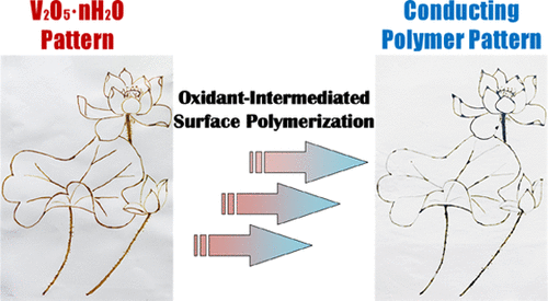
Conducting polymer coatings and patterns are the most important forms of these materials for many practical applications, but a simple and efficient approach to these forms remains challenging. Herein, we report a universal oxidant-intermediated surface polymerization (OISP) for the fabrication of conducting polymer coatings and patterns on various substrates. A coating or pattern composed of densely packed colloidal V2O5·nH2O nanowires is deposited on the substrate via spin coating, dip coating, or printing, which is converted into a conducting polymer one after in situ oxidation polymerization. The polymerization occurs selectively on the V2O5·nH2O coatings, and high-quality polypyrrole, polyaniline, and poly(3,4-ethylenedioxythiophene) coatings and patterns on planar and curved polymeric, metallic, and ceramic substrates are obtained in a fast reaction rate similar to the electrochemical polymerization. The mechanistic study reveals that the method relies on the excellent processability and formability of V2O5·nH2O nanowires, which is further explained by their large aspect ratio and surface activity. A flexible gas sensor array comprising three individual sensors made of different conducting polymers is fabricated using oxidant-intermediated surface polymerization, and it is successfully used to distinguish various analyte vapors. The method developed here will provide a powerful tool for the fabrication of conducting polymer-based devices.
中文翻译:

多种基材上的连续且有图案的导电聚合物涂层:通过氧化剂介导的表面聚合快速制备及其在柔性器件中的应用
对于许多实际应用而言,导电聚合物涂层和图案是这些材料最重要的形式,但是对这些形式进行简单有效的方法仍然具有挑战性。在这里,我们报告了一种通用的氧化剂介导的表面聚合(OISP),用于在各种基材上制造导电聚合物涂层和图案。由紧密堆积的胶体V 2 O 5 · n H 2 O纳米线组成的涂层或图案通过旋涂,浸涂或印刷沉积在基材上,在原位氧化聚合反应后转化为导电聚合物。聚合选择性地发生在V 2 O上在平面和弯曲的聚合物,金属和陶瓷基材上,可以以类似于电化学的快速反应速率获得5 · n H 2 O涂层以及高质量的聚吡咯,聚苯胺和聚(3,4-乙撑二氧噻吩)涂层和图案聚合。机理研究表明,该方法依赖于V 2 O 5 · n H 2的优异加工性能和可成形性。O纳米线,其宽高比和表面活性得到进一步解释。使用氧化剂介导的表面聚合技术制造了一个柔性气体传感器阵列,该阵列包括三个由不同导电聚合物制成的独立传感器,并且已成功用于区分各种分析物蒸气。此处开发的方法将为制造导电聚合物基器件提供强大的工具。
更新日期:2021-02-03
中文翻译:
多种基材上的连续且有图案的导电聚合物涂层:通过氧化剂介导的表面聚合快速制备及其在柔性器件中的应用
对于许多实际应用而言,导电聚合物涂层和图案是这些材料最重要的形式,但是对这些形式进行简单有效的方法仍然具有挑战性。在这里,我们报告了一种通用的氧化剂介导的表面聚合(OISP),用于在各种基材上制造导电聚合物涂层和图案。由紧密堆积的胶体V 2 O 5 · n H 2 O纳米线组成的涂层或图案通过旋涂,浸涂或印刷沉积在基材上,在原位氧化聚合反应后转化为导电聚合物。聚合选择性地发生在V 2 O上在平面和弯曲的聚合物,金属和陶瓷基材上,可以以类似于电化学的快速反应速率获得5 · n H 2 O涂层以及高质量的聚吡咯,聚苯胺和聚(3,4-乙撑二氧噻吩)涂层和图案聚合。机理研究表明,该方法依赖于V 2 O 5 · n H 2的优异加工性能和可成形性。O纳米线,其宽高比和表面活性得到进一步解释。使用氧化剂介导的表面聚合技术制造了一个柔性气体传感器阵列,该阵列包括三个由不同导电聚合物制成的独立传感器,并且已成功用于区分各种分析物蒸气。此处开发的方法将为制造导电聚合物基器件提供强大的工具。


 京公网安备 11010802027423号