当前位置:
X-MOL 学术
›
ACS Appl. Mater. Interfaces
›
论文详情
Our official English website, www.x-mol.net, welcomes your feedback! (Note: you will need to create a separate account there.)
Photophysical Dynamics in Semiconducting Graphene Quantum Dots Integrated with 2D MoS2 for Optical Enhancement in the Near UV
ACS Applied Materials & Interfaces ( IF 9.5 ) Pub Date : 2021-01-20 , DOI: 10.1021/acsami.0c18615 Misook Min 1 , Shambhavi Sakri 1 , Gustavo A. Saenz 2 , Anupama B. Kaul 1, 2
ACS Applied Materials & Interfaces ( IF 9.5 ) Pub Date : 2021-01-20 , DOI: 10.1021/acsami.0c18615 Misook Min 1 , Shambhavi Sakri 1 , Gustavo A. Saenz 2 , Anupama B. Kaul 1, 2
Affiliation
|
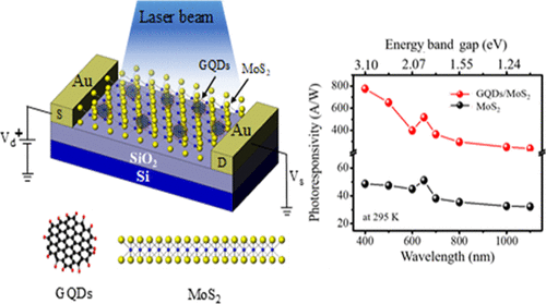
The hybrid structure of zero-dimensional (0D) graphene quantum dots (GQDs) and semiconducting two-dimensional (2D) MoS2 has been investigated, which exhibit outstanding properties for optoelectronic devices surpassing the limitations of MoS2 photodetectors where the GQDs extend the optical absorption into the near-UV regime. The GQDs and MoS2 films are characterized by Raman and photoluminescence (PL) spectroscopies, along with atomic force microscopy. After outlining the fabrication of our 0D–2D heterostructure photodetectors comprising GQDs with bulk MoS2 sheets, their photoresponse to the incoming radiation was measured. The hybrid GQD/MoS2 heterostructure photodetector exhibits a high photoresponsivity R of more than 1200 A W–1 at 0.64 mW/cm2 at room temperature T. The T-dependent optoelectronic measurements revealed a peak R of ∼544 A W–1 at 245 K, examined from 5.4 K up to 305 K with an incoming white light power density of 3.2 mW/cm2. A tunable laser revealed the photocurrent to be maximal at lower wavelengths in the near ultraviolet (UV) over the 400–1100 nm spectral range, where the R of the hybrid GQDs/MoS2 was ∼775 A W–1, while a value of 2.33 × 10¹² Jones was computed for the detectivity D* at 400 nm. The external quantum efficiency was measured to be ∼99.8% at 650 nm, which increased to 241% when the wavelength of the incoming laser was reduced to 400 nm. Time-resolved measurements of the photocurrent for the hybrid devices resulted in a rise time τrise and a fall time τfall of ∼7 and ∼25 ms, respectively, at room T, which are 10× lower compared to previous reports. From our promising results, we conclude that the GQDs exhibit a sizable band gap upon optical excitation, where photocarriers are injected into the MoS2 films, endowing the hybrids with long carrier lifetimes to enable efficient light absorption beyond the visible and into the near-UV regime. The GQD–MoS2 structure is thus an enabling platform for high-performance photodetectors, optoelectronic circuits, and quantum devices.
中文翻译:

半导体石墨烯量子点中集成2D MoS 2的光物理动力学,用于近紫外光增强
已经研究了零维(0D)石墨烯量子点(GQDs)和半导体二维(2D)MoS 2的混合结构,它们显示出超越MoS 2光电探测器的局限性的光电器件优异的性能,其中GQD扩展了光学吸收到近紫外线区域。GQD和MoS 2薄膜的特征在于拉曼光谱和光致发光(PL)光谱,以及原子力显微镜。在概述了我们的0D–2D异质结构光电探测器(包括带有大量MoS 2片的GQD)的制造后,测量了它们对入射辐射的光响应。混合GQD / MoS 2异质结构光电探测器具有高光响应性在室温T下,在0.64 mW / cm 2时,R大于1200 AW –1。所述Ť依赖性光电子测量表明峰值ř ~544 AW的-1在245 K,从5.4ķ向上检查,以305 K的3.2毫瓦/平方厘米的进入的白光的功率密度2。可调激光器显示,在400-1100 nm光谱范围内,在近紫外(UV)的较低波长处,光电流最大,其中混合GQDs / MoS 2的R为〜775 AW –1,而值为2.33 ×10 12 Jones被计算出探测灵敏度D*在400 nm处。在650 nm处测得的外部量子效率为〜99.8%,当入射激光的波长减小到400 nm时,外部量子效率增加到241%。光电流对混合设备的时间分辨的测量导致的上升时间τ上升和下降时间τ下降的~7和〜25毫秒,分别在室温Ť,10×下相比以前的报告它们。从我们有希望的结果中,我们得出结论,GQD在光激发时会显示出相当大的带隙,其中将光载流子注入MoS 2薄膜中,使杂化体具有较长的载流子寿命,从而能够有效吸收可见光和近紫外光政权。GQD–MoS 2 因此,该结构是高性能光电探测器,光电电路和量子设备的使能平台。
更新日期:2021-02-03
中文翻译:
半导体石墨烯量子点中集成2D MoS 2的光物理动力学,用于近紫外光增强
已经研究了零维(0D)石墨烯量子点(GQDs)和半导体二维(2D)MoS 2的混合结构,它们显示出超越MoS 2光电探测器的局限性的光电器件优异的性能,其中GQD扩展了光学吸收到近紫外线区域。GQD和MoS 2薄膜的特征在于拉曼光谱和光致发光(PL)光谱,以及原子力显微镜。在概述了我们的0D–2D异质结构光电探测器(包括带有大量MoS 2片的GQD)的制造后,测量了它们对入射辐射的光响应。混合GQD / MoS 2异质结构光电探测器具有高光响应性在室温T下,在0.64 mW / cm 2时,R大于1200 AW –1。所述Ť依赖性光电子测量表明峰值ř ~544 AW的-1在245 K,从5.4ķ向上检查,以305 K的3.2毫瓦/平方厘米的进入的白光的功率密度2。可调激光器显示,在400-1100 nm光谱范围内,在近紫外(UV)的较低波长处,光电流最大,其中混合GQDs / MoS 2的R为〜775 AW –1,而值为2.33 ×10 12 Jones被计算出探测灵敏度D*在400 nm处。在650 nm处测得的外部量子效率为〜99.8%,当入射激光的波长减小到400 nm时,外部量子效率增加到241%。光电流对混合设备的时间分辨的测量导致的上升时间τ上升和下降时间τ下降的~7和〜25毫秒,分别在室温Ť,10×下相比以前的报告它们。从我们有希望的结果中,我们得出结论,GQD在光激发时会显示出相当大的带隙,其中将光载流子注入MoS 2薄膜中,使杂化体具有较长的载流子寿命,从而能够有效吸收可见光和近紫外光政权。GQD–MoS 2 因此,该结构是高性能光电探测器,光电电路和量子设备的使能平台。


 京公网安备 11010802027423号