当前位置:
X-MOL 学术
›
Adv. Electron. Mater.
›
论文详情
Our official English website, www.x-mol.net, welcomes your
feedback! (Note: you will need to create a separate account there.)
Solvent‐Free Coating of Organic Semiconductor Membranes with Centimetric Crystalline Domains
Advanced Electronic Materials ( IF 5.3 ) Pub Date : 2021-01-21 , DOI: 10.1002/aelm.202000792 Yu Xia 1 , Ruipeng Li 2 , Esther Tsai 3 , Yaowu He 4 , Tianran Liu 5 , Xiaoming Zhao 1 , Kaichen Gu 1 , Hong Meng 4 , Yueh‐Lin Loo 1, 6
Advanced Electronic Materials ( IF 5.3 ) Pub Date : 2021-01-21 , DOI: 10.1002/aelm.202000792 Yu Xia 1 , Ruipeng Li 2 , Esther Tsai 3 , Yaowu He 4 , Tianran Liu 5 , Xiaoming Zhao 1 , Kaichen Gu 1 , Hong Meng 4 , Yueh‐Lin Loo 1, 6
Affiliation
|
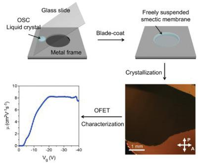
Organic semiconductors (OSCs) have shown great promise in a variety of applications. Although solution processing of OSCs has resulted in high‐quality films, exquisite control of structural development to minimize defect formation during large‐scale fabrication remains formidable. Compounding this challenge is the use of halogenated organic solvents, which poses significant health and environmental hazards. However, the solvent‐free techniques introduced thus far impose additional limitations on solidification kinetics; the resulting OSC thin films are often more defective than those processed from solution. Here, a solvent‐free technique is reported to prepare OSC membranes with centimetric crystalline domains. Leveraging the tendency for liquid crystalline materials to preferentially orient, OSCs are “prealigned” by depositing them from the melt over a metal frame to form a freely suspended membrane. Crystallization from this prealigned phase affords membranes with unprecedented structural order across macroscopic distances. Field‐effect transistors comprising membranes of dioctyl[1]‐benzothieno[3,2‐b][1]benzothiophene (C8BTBT) and didodecyl[1]‐benzothieno[3,2‐b][1]benzothiophene (C12BTBT) having centimeter‐sized domains as active layers exhibit a hole mobility of ≈8.6 cm2 V−1 s−1, superseding the mobility of any transistors whose active layers are deposited from melt. This technique is scalable to yield membranes with large crystalline domains over wafer dimensions, making it amenable for broad applications in large‐area organic electronics.
中文翻译:

具有厘米结晶域的有机半导体膜的无溶剂涂层
有机半导体(OSC)在各种应用中都显示出了广阔的前景。尽管OSC的固溶处理已产生了高质量的薄膜,但是对结构开发的精确控制以最大程度地减少大规模制造过程中的缺陷形成仍然很艰巨。使用卤代有机溶剂使这一挑战更加复杂,这对健康和环境构成了重大危害。但是,迄今为止引入的无溶剂技术对固化动力学施加了其他限制。所得的OSC薄膜通常比从溶液中处理的薄膜更具缺陷性。在这里,据报道使用无溶剂技术来制备具有厘米级晶畴的OSC膜。利用液晶材料优先取向的趋势,通过从熔体中将OSC沉积在金属框架上以形成自由悬浮的膜,从而对其进行“预对齐”。从该预取向相的结晶使膜在宏观距离上具有空前的结构顺序。包含具有厘米的二辛基[1]-苯并噻吩并[3,2-b] [1]苯并噻吩(C8BTBT)和双十二烷基[1]-苯并噻吩并[3,2-b] [1]苯并噻吩(C12BTBT)膜的场效应晶体管尺寸大小的区域作为有源层,其空穴迁移率约为8.6 cm2 V -1 s -1,取代了其有源层是由熔体沉积的任何晶体管的迁移率。此技术可扩展以生产在晶片尺寸上具有大晶畴的膜,使其适合在大面积有机电子产品中的广泛应用。
更新日期:2021-03-11
中文翻译:
具有厘米结晶域的有机半导体膜的无溶剂涂层
有机半导体(OSC)在各种应用中都显示出了广阔的前景。尽管OSC的固溶处理已产生了高质量的薄膜,但是对结构开发的精确控制以最大程度地减少大规模制造过程中的缺陷形成仍然很艰巨。使用卤代有机溶剂使这一挑战更加复杂,这对健康和环境构成了重大危害。但是,迄今为止引入的无溶剂技术对固化动力学施加了其他限制。所得的OSC薄膜通常比从溶液中处理的薄膜更具缺陷性。在这里,据报道使用无溶剂技术来制备具有厘米级晶畴的OSC膜。利用液晶材料优先取向的趋势,通过从熔体中将OSC沉积在金属框架上以形成自由悬浮的膜,从而对其进行“预对齐”。从该预取向相的结晶使膜在宏观距离上具有空前的结构顺序。包含具有厘米的二辛基[1]-苯并噻吩并[3,2-b] [1]苯并噻吩(C8BTBT)和双十二烷基[1]-苯并噻吩并[3,2-b] [1]苯并噻吩(C12BTBT)膜的场效应晶体管尺寸大小的区域作为有源层,其空穴迁移率约为8.6 cm2 V -1 s -1,取代了其有源层是由熔体沉积的任何晶体管的迁移率。此技术可扩展以生产在晶片尺寸上具有大晶畴的膜,使其适合在大面积有机电子产品中的广泛应用。


 京公网安备 11010802027423号