当前位置:
X-MOL 学术
›
Adv. Mater.
›
论文详情
Our official English website, www.x-mol.net, welcomes your
feedback! (Note: you will need to create a separate account there.)
Direct Synthesis and Enhanced Rectification of Alloy‐to‐Alloy 2D Type‐II MoS2(1‐x)Se2x/SnS2(1‐y)Se2y Heterostructures
Advanced Materials ( IF 27.4 ) Pub Date : 2021-01-14 , DOI: 10.1002/adma.202006908 Xiaoting Wang 1, 2 , Longfei Pan 1, 2 , Juehan Yang 1 , Bo Li 3 , Yue‐Yang Liu 1 , Zhongming Wei 1, 2
Advanced Materials ( IF 27.4 ) Pub Date : 2021-01-14 , DOI: 10.1002/adma.202006908 Xiaoting Wang 1, 2 , Longfei Pan 1, 2 , Juehan Yang 1 , Bo Li 3 , Yue‐Yang Liu 1 , Zhongming Wei 1, 2
Affiliation
|
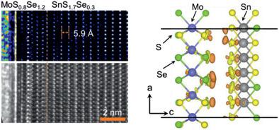
The interfacial tunable band alignment of heterostructures is coveted in device design and optimization of device performance. As an intentional approach, alloying allows band engineering and continuous band‐edge tunability for low‐dimensional semiconductors. Thus, combining the tunability of alloying with the band structure of a heterostructure is highly desirable for the improvement of device characteristics. In this work, the single‐step growth of alloy‐to‐alloy (MoS2(1‐x)Se2x/SnS2(1‐y)Se2y) 2D vertical heterostructures is demonstrated. Electron diffraction reveals the well‐aligned heteroepitaxial relationship for the heterostructure, and a near‐atomically sharp and defect‐free boundary along the interface is observed. The nearly intrinsic van der Waals (vdW) interface enables measurement of the intrinsic behaviors of the heterostructures. The optimized type‐II band alignment for the MoS2(1‐x)Se2x/SnS2(1‐y)Se2y heterostructure, along with the large band offset and effective charge transfer, is confirmed through quenched PL spectroscopy combined with density functional theory calculations. Devices based on completely stacked heterostructures show one or two orders enhanced electron mobility and rectification ratio than those of the constituent materials. The realization of device‐quality alloy‐to‐alloy heterostructures provides a new material platform for precisely tuning band alignment and optimizing device applications.
中文翻译:

合金-合金2D Type-II MoS2(1-x)Se2x / SnS2(1-y)Se2y异质结构的直接合成和增强精馏
异质结构的界面可调带对准在器件设计和器件性能优化中令人垂涎。作为一种有意的方法,合金化可以为低维半导体提供能带工程和连续的带边可调性。因此,非常需要将合金化的可调性与异质结构的能带结构相结合,以改善器件特性。在这项工作中,合金到合金(MoS 2(1- x) Se 2 x / SnS 2(1- y) Se 2 y)的单步生长)展示了二维垂直异质结构。电子衍射揭示了异质结构的良好排列的异质外延关系,并且沿界面观察到接近原子的清晰无缺陷的边界。接近内在的范德华(vdW)界面可测量异质结构的内在行为。MoS 2(1- x) Se 2 x / SnS 2(1- y) Se 2 y的优化II型谱带对准通过淬灭PL光谱结合密度泛函理论计算,证实了异质结构以及大的带偏移和有效的电荷转移。基于完全堆叠的异质结构的器件显示出比组成材料的电子迁移率和整流比提高一到两个数量级。器件质量的合金到合金异质结构的实现为精确调整能带对准和优化器件应用提供了新的材料平台。
更新日期:2021-02-22
中文翻译:
合金-合金2D Type-II MoS2(1-x)Se2x / SnS2(1-y)Se2y异质结构的直接合成和增强精馏
异质结构的界面可调带对准在器件设计和器件性能优化中令人垂涎。作为一种有意的方法,合金化可以为低维半导体提供能带工程和连续的带边可调性。因此,非常需要将合金化的可调性与异质结构的能带结构相结合,以改善器件特性。在这项工作中,合金到合金(MoS 2(1- x) Se 2 x / SnS 2(1- y) Se 2 y)的单步生长)展示了二维垂直异质结构。电子衍射揭示了异质结构的良好排列的异质外延关系,并且沿界面观察到接近原子的清晰无缺陷的边界。接近内在的范德华(vdW)界面可测量异质结构的内在行为。MoS 2(1- x) Se 2 x / SnS 2(1- y) Se 2 y的优化II型谱带对准通过淬灭PL光谱结合密度泛函理论计算,证实了异质结构以及大的带偏移和有效的电荷转移。基于完全堆叠的异质结构的器件显示出比组成材料的电子迁移率和整流比提高一到两个数量级。器件质量的合金到合金异质结构的实现为精确调整能带对准和优化器件应用提供了新的材料平台。


 京公网安备 11010802027423号