当前位置:
X-MOL 学术
›
Adv. Electron. Mater.
›
论文详情
Our official English website, www.x-mol.net, welcomes your
feedback! (Note: you will need to create a separate account there.)
Characterization of Aerosol Deposited Cesium Lead Tribromide Perovskite Films on Interdigited ITO Electrodes
Advanced Electronic Materials ( IF 5.3 ) Pub Date : 2021-01-15 , DOI: 10.1002/aelm.202001165 Albert These 1, 2 , Neamul H. Khansur 3 , Osbel Almora 1, 2, 4 , Larry Luer 1 , Gebhard J. Matt 1 , Udo Eckstein 3 , Anastasia Barabash 1 , Andres Osvet 1 , Kyle G. Webber 3 , Christoph J. Brabec 1
Advanced Electronic Materials ( IF 5.3 ) Pub Date : 2021-01-15 , DOI: 10.1002/aelm.202001165 Albert These 1, 2 , Neamul H. Khansur 3 , Osbel Almora 1, 2, 4 , Larry Luer 1 , Gebhard J. Matt 1 , Udo Eckstein 3 , Anastasia Barabash 1 , Andres Osvet 1 , Kyle G. Webber 3 , Christoph J. Brabec 1
Affiliation
|
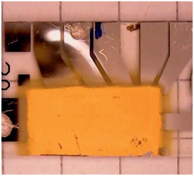
Aerosol deposition (AD) is a promising additive manufacturing method to fabricate low‐cost, scalable films at room temperature, but has not been considered for semiconductor processing, so far. The successful preparation of cesium lead tribromide (CsPbBr3) perovskite films on interdigitated indium tin oxide (ITO) electrodes by means of AD is reported here. The 20–35 µm thick layers are dense and have good adhesion to the substrate. The orthorhombic Pnma crystal structure of the precursor powder was retained during the deposition process with no signs of defect formation. The formation of electronic defects by photoluminescence spectroscopy is investigated and found slightly increased carrier recombination from defect sites for AD films compared to the powder. A nonuniform defect distribution across the layer, presumably induced by the impact of the semiconducting grains on the hard substrate surface, is revealed. The opto‐electronic properties of AD processed semiconducting films is further tested by electrical measurements and confirmed good semiconducting properties and high responsivity for the films. These results demonstrate that AD processing of metal halide perovskites is possible for opto‐electronic device manufacturing on 3D surfaces. It is believed that this work paves the way for the fabrication of previously unimaginable opto‐electronic devices by additive manufacturing.
中文翻译:

叉指式ITO电极上气溶胶沉积三溴化铯铅钙钛矿薄膜的表征
气溶胶沉积(AD)是一种有前途的增材制造方法,可以在室温下制造低成本,可缩放的薄膜,但迄今为止尚未被考虑用于半导体工艺。本文报道了通过AD成功地在叉指状铟锡氧化物(ITO)电极上成功制备了三溴化铯铯(CsPbBr 3)钙钛矿薄膜。20–35 µm厚的层很致密,对基材具有良好的附着力。斜方晶状体在沉积过程中保留了前体粉末的晶体结构,没有缺陷形成的迹象。对通过光致发光光谱法形成的电子缺陷进行了研究,发现与粉末相比,AD膜缺陷部位的载流子重组略有增加。揭示了整个层上的不均匀缺陷分布,这大概是由半导电晶粒在硬质基材表面上的撞击所引起的。通过电测量进一步测试了经过AD处理的半导体薄膜的光电性能,并证实了该薄膜具有良好的半导体性能和高响应性。这些结果表明,金属卤化物钙钛矿的AD处理对于在3D表面上制造光电设备是可能的。
更新日期:2021-03-11
中文翻译:
叉指式ITO电极上气溶胶沉积三溴化铯铅钙钛矿薄膜的表征
气溶胶沉积(AD)是一种有前途的增材制造方法,可以在室温下制造低成本,可缩放的薄膜,但迄今为止尚未被考虑用于半导体工艺。本文报道了通过AD成功地在叉指状铟锡氧化物(ITO)电极上成功制备了三溴化铯铯(CsPbBr 3)钙钛矿薄膜。20–35 µm厚的层很致密,对基材具有良好的附着力。斜方晶状体在沉积过程中保留了前体粉末的晶体结构,没有缺陷形成的迹象。对通过光致发光光谱法形成的电子缺陷进行了研究,发现与粉末相比,AD膜缺陷部位的载流子重组略有增加。揭示了整个层上的不均匀缺陷分布,这大概是由半导电晶粒在硬质基材表面上的撞击所引起的。通过电测量进一步测试了经过AD处理的半导体薄膜的光电性能,并证实了该薄膜具有良好的半导体性能和高响应性。这些结果表明,金属卤化物钙钛矿的AD处理对于在3D表面上制造光电设备是可能的。


 京公网安备 11010802027423号