Electronic Materials Letters ( IF 2.1 ) Pub Date : 2021-01-13 , DOI: 10.1007/s13391-020-00263-8 Gil Su Jang , Du Yun Kim , Nong-Moon Hwang
|
Abstract
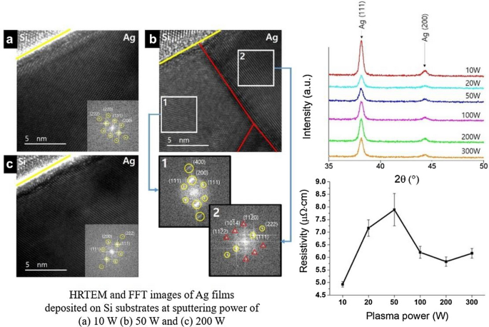
Effects of sputtering power on the deposition rate and microstructure, crystallinity, and electrical properties of Ag films during direct current (DC) magnetron sputtering are investigated. Thin films (~ 100 nm) are deposited at sputtering powers of 10, 20, 50, 100, 200 and 300 W and analyzed by field-emission scanning electron microscopy (FESEM), X-ray diffraction (XRD), transmission electron microscopy (TEM) and a four-point probe. The film deposited at a sputtering power of 10 W has the lowest growth rate, but the highest crystalline quality, with the lowest full width at half maximum (FWHM) and the lowest resistivity. The film deposited at a sputtering power of 200 W has the highest growth rate, and the second best crystalline quality in view of FWHM and resistivity. The film deposited at a sputtering power of 50 W has the moderate growth rate, and the worst crystalline quality in view of FWHM and resistivity. High-resolution TEM observations reveal that films deposited at sputtering powers of 10 and 200 W have far fewer defects, such as grain boundaries, dislocations and stacking faults than those deposited at a sputtering power of 50 W. Such deposition behavior could be explained by sputtering power, which affected the generation of the charged nanoparticles. And the high quality of films could be obtained at a high deposition rate, in which charge plays an important role.
Graphic Abstract
中文翻译:
直流磁控溅射过程中带电纳米粒子的生成行为和Ag薄膜的生长对溅射功率的影响
摘要
研究了直流磁控溅射过程中溅射功率对Ag膜沉积速率和微观结构,结晶度以及电学性质的影响。以10、20、50、100、200和300 W的溅射功率沉积薄膜(〜100 nm),并通过场发射扫描电子显微镜(FESEM),X射线衍射(XRD),透射电子显微镜( TEM)和四点探针。以10 W的溅射功率沉积的薄膜具有最低的生长速率,但具有最高的晶体质量,具有最低的半峰全宽(FWHM)和最低的电阻率。考虑到FWHM和电阻率,以200W的溅射功率沉积的膜具有最高的生长速率和次之的结晶质量。以50 W的溅射功率沉积的薄膜具有中等的生长速率,考虑到半高宽和电阻率,晶体质量最差。高分辨率TEM观察表明,与以50 W的溅射功率沉积的薄膜相比,以10和200 W的溅射功率沉积的薄膜具有更少的缺陷,例如晶界,位错和堆垛层错。这种沉积行为可以通过溅射来解释。功率,这会影响带电纳米粒子的产生。而且可以以高沉积速率获得高质量的薄膜,其中电荷起着重要的作用。可以通过溅射功率来解释这种沉积行为,溅射功率会影响带电纳米粒子的产生。而且可以以高沉积速率获得高质量的薄膜,其中电荷起着重要的作用。可以通过溅射功率来解释这种沉积行为,溅射功率会影响带电纳米粒子的产生。而且可以以高沉积速率获得高质量的薄膜,其中电荷起着重要的作用。


 京公网安备 11010802027423号