当前位置:
X-MOL 学术
›
Adv. Electron. Mater.
›
论文详情
Our official English website, www.x-mol.net, welcomes your
feedback! (Note: you will need to create a separate account there.)
Trap Reduction through O3 Post‐Deposition Treatment of Y2O3 Thin Films Grown by Atomic Layer Deposition on Ge Substrates
Advanced Electronic Materials ( IF 5.3 ) Pub Date : 2021-01-12 , DOI: 10.1002/aelm.202000819 Dong Gun Kim 1 , Dae Seon Kwon 1 , Junil Lim 1 , Haengha Seo 1 , Tae Kyun Kim 1 , Woongkyu Lee 2 , Cheol Seong Hwang 1
Advanced Electronic Materials ( IF 5.3 ) Pub Date : 2021-01-12 , DOI: 10.1002/aelm.202000819 Dong Gun Kim 1 , Dae Seon Kwon 1 , Junil Lim 1 , Haengha Seo 1 , Tae Kyun Kim 1 , Woongkyu Lee 2 , Cheol Seong Hwang 1
Affiliation
|
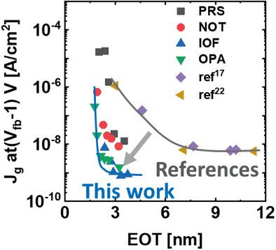
For Ge‐based metal‐oxide‐semiconductor field‐effect transistor application, high‐k Y2O3 thin films are deposited on Ge single‐crystal substrate using atomic layer deposition. The primary drawbacks of a metal‐oxide‐semiconductor capacitor with pristine Y2O3 are large hysteresis and high leakage current. Through forming gas annealing (FGA), the leakage current can be reduced by approximately three orders of magnitude, along with the reduction of interface trap density. However, there is still a large hysteresis in the capacitance–voltage curves. O3 post‐deposition annealing (OPA) is used to solve the problem. The formation of the YGeOx interfacial layer through OPA and the reduction of the defect level of the Y2O3 thin film effectively decrease the hysteresis, which also decreases the leakage current. Additionally, the hysteresis is 690 mV when only FGA is performed. However, it is further reduced to 260 mV through OPA. Moreover, the remote oxygen scavenging effect using TiN/Pt electrodes prevents an unintentional increase in equivalent oxide thickness (EOT). The 4.7 nm thick Y2O3 film results in an EOT of 1.77 nm and leakage current density of 2.1 × 10⁻⁷ A cm−2 (at flat band voltage—1 V) after the OPA.
中文翻译:

Ge基体上原子层沉积生长的Y2O3薄膜的O3后沉积处理减少陷阱
对于基于Ge的金属氧化物半导体场效应晶体管,应使用原子层沉积法将高k Y 2 O 3薄膜沉积在Ge单晶衬底上。原始Y 2 O 3的金属氧化物半导体电容器的主要缺点是磁滞大和漏电流大。通过形成气体退火(FGA),可以将泄漏电流降低大约三个数量级,同时降低界面陷阱密度。但是,电容-电压曲线仍存在较大的滞后现象。O 3沉积后退火(OPA)用于解决该问题。YGeO x的形成通过OPA的界面层和Y 2 O 3薄膜的缺陷水平的降低有效地减小了磁滞,这也减小了漏电流。此外,仅执行FGA时的迟滞为690 mV。但是,通过OPA可以将其进一步降低至260 mV。此外,使用TiN / Pt电极的远程除氧效果可防止意外增加等效氧化物厚度(EOT)。厚度为4.7 nm的Y 2 O 3膜在OPA之后产生的EOT为1.77 nm,泄漏电流密度为2.1×10 -7 A cm -2(在平带电压为1 V时)。
更新日期:2021-02-15
中文翻译:
Ge基体上原子层沉积生长的Y2O3薄膜的O3后沉积处理减少陷阱
对于基于Ge的金属氧化物半导体场效应晶体管,应使用原子层沉积法将高k Y 2 O 3薄膜沉积在Ge单晶衬底上。原始Y 2 O 3的金属氧化物半导体电容器的主要缺点是磁滞大和漏电流大。通过形成气体退火(FGA),可以将泄漏电流降低大约三个数量级,同时降低界面陷阱密度。但是,电容-电压曲线仍存在较大的滞后现象。O 3沉积后退火(OPA)用于解决该问题。YGeO x的形成通过OPA的界面层和Y 2 O 3薄膜的缺陷水平的降低有效地减小了磁滞,这也减小了漏电流。此外,仅执行FGA时的迟滞为690 mV。但是,通过OPA可以将其进一步降低至260 mV。此外,使用TiN / Pt电极的远程除氧效果可防止意外增加等效氧化物厚度(EOT)。厚度为4.7 nm的Y 2 O 3膜在OPA之后产生的EOT为1.77 nm,泄漏电流密度为2.1×10 -7 A cm -2(在平带电压为1 V时)。


 京公网安备 11010802027423号