Catalysis Today ( IF 5.2 ) Pub Date : 2021-01-12 , DOI: 10.1016/j.cattod.2020.12.034 Wei Hu , Fengjuan Si , Hongtao Xue , Fuling Tang , Wensheng Li
|
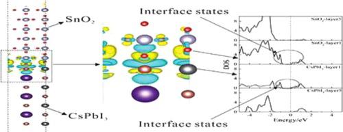
Crystal structure and photoelectric properties of the light absorbing layer (CsPbI3)/electron transporting layer (SnO2) heterogeneous interface were studied at the atomic and electronic levels by using the first principles calculations. The calculation of electronic band structure indicates that band gap of the cubic CsPbI3 is about 1.48 eV. The lattice mismatch of SnO2 (110)/CsPbI3 (100) interface is 4.45 % and the interface binding energy is -2.86 J/m2. Due to the contribution of I-5p, Pb-6p, Pb-6s, and O-2p orbitals with the CsPbI3 (100) layer1 and SnO2 (110) layer1, the SnO2 (110)/CsPbI3 (100) interface exhibits some new electronic density of states nearby the Fermi level. The static dielectric constant of crystal CsPbI3 is 6.22, and its optical band gap is also approximate 1.48 eV.
中文翻译:
SnO 2 /CsPbI 3界面的电子和光学特性:使用第一性原理计算
通过使用第一性原理计算,在原子和电子水平上研究了光吸收层(CsPbI 3)/电子传输层(SnO 2)异质界面的晶体结构和光电特性。电子能带结构的计算表明立方CsPbI 3 的带隙约为1.48 eV。SnO 2 (110)/CsPbI 3 (100) 界面的晶格失配为4.45%,界面结合能为-2.86 J/m 2。由于 I-5 p、Pb-6 p、Pb-6 s和 O-2 p轨道与 CsPbI 3 (100) 层 1 和 SnO的贡献在图 2 (110) 层 1 中,SnO 2 (110)/CsPbI 3 (100) 界面在费米能级附近表现出一些新的电子态密度。晶体CsPbI 3的静态介电常数为6.22,其光学带隙也约为1.48 eV。


 京公网安备 11010802027423号