Microelectronic Engineering ( IF 2.6 ) Pub Date : 2021-01-07 , DOI: 10.1016/j.mee.2021.111505 Zhixiang Liu , Yunqing Tang
|
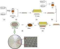
Fixed abrasive polishing pad plays an important role in planarization of the surface of integrated circuit and semiconductor substrate. This paper reports a systematic approach for fabricating the pad using polyurethane, metal mold and layer-by-layer curing without binders. The pad surface with uniformly and orderly arranged convexities is undamaged during the fabrication process. Because of using prepolymer with hydrophobic groups, self-conditioning, stable polishing process and no water swelling are observed during the polishing process. The experimental results show the material removal rate is 72.972 nm/min and the polished surface roughness is 0.007 μm for SiC wafer. It builds a basis for high efficient preparation technology on hydrophobic fixed abrasive pad.
中文翻译:
一种基于层层法的疏水性固定磨料垫的方法
固定式磨料抛光垫在集成电路和半导体衬底表面的平面化中起着重要作用。本文报道了一种使用聚氨酯,金属模具和不使用粘合剂的逐层固化方法制造衬垫的系统方法。在制造过程中,具有均匀且有序排列的凸面的焊盘表面没有损坏。由于使用具有疏水基团的预聚物,因此在抛光过程中不会出现自我调节,稳定的抛光过程且没有水溶胀的现象。实验结果表明,SiC晶片的材料去除速率为72.972 nm / min,抛光表面粗糙度为0.007μm。它为疏水固定磨料垫上的高效制备技术奠定了基础。


 京公网安备 11010802027423号