Our official English website, www.x-mol.net, welcomes your
feedback! (Note: you will need to create a separate account there.)
Band Structure Extraction at Hybrid Narrow‐Gap Semiconductor–Metal Interfaces
Advanced Science ( IF 14.3 ) Pub Date : 2020-12-31 , DOI: 10.1002/advs.202003087 Sergej Schuwalow 1 , Niels B M Schröter 2 , Jan Gukelberger 3 , Candice Thomas 4, 5 , Vladimir Strocov 2 , John Gamble 3 , Alla Chikina 2 , Marco Caputo 2 , Jonas Krieger 2 , Geoffrey C Gardner 4 , Matthias Troyer 3 , Gabriel Aeppli 2, 6, 7 , Michael J Manfra 4, 5, 8 , Peter Krogstrup 1
Advanced Science ( IF 14.3 ) Pub Date : 2020-12-31 , DOI: 10.1002/advs.202003087 Sergej Schuwalow 1 , Niels B M Schröter 2 , Jan Gukelberger 3 , Candice Thomas 4, 5 , Vladimir Strocov 2 , John Gamble 3 , Alla Chikina 2 , Marco Caputo 2 , Jonas Krieger 2 , Geoffrey C Gardner 4 , Matthias Troyer 3 , Gabriel Aeppli 2, 6, 7 , Michael J Manfra 4, 5, 8 , Peter Krogstrup 1
Affiliation
|
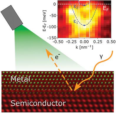
The design of epitaxial semiconductor–superconductor and semiconductor–metal quantum devices requires a detailed understanding of the interfacial electronic band structure. However, the band alignment of buried interfaces is difficult to predict theoretically and to measure experimentally. This work presents a procedure that allows to reliably determine critical parameters for engineering quantum devices; band offset, band bending profile, and number of occupied quantum well subbands of interfacial accumulation layers at semiconductor‐metal interfaces. Soft X‐ray angle‐resolved photoemission is used to directly measure the quantum well states as well as valence bands and core levels for the InAs(100)/Al interface, an important platform for Majorana‐zero‐mode based topological qubits, and demonstrate that the fabrication process strongly influences the band offset, which in turn controls the topological phase diagrams. Since the method is transferable to other narrow gap semiconductors, it can be used more generally for engineering semiconductor–metal and semiconductor–superconductor interfaces in gate‐tunable superconducting devices.
中文翻译:

混合窄带隙半导体-金属界面的能带结构提取
外延半导体-超导体和半导体-金属量子器件的设计需要详细了解界面电子能带结构。然而,掩埋界面的能带排列很难在理论上预测和在实验上测量。这项工作提出了一种程序,可以可靠地确定工程量子设备的关键参数;能带偏移、能带弯曲轮廓以及半导体-金属界面处界面积累层的占据量子阱子带的数量。软X射线角分辨光电子发射用于直接测量InAs(100)/Al界面的量子阱态以及价带和核心能级,这是基于马约拉纳零模式的拓扑量子位的重要平台,并证明制造工艺强烈影响能带偏移,进而控制拓扑相图。由于该方法可转移到其他窄带隙半导体,因此它可以更广泛地用于栅极可调超导器件中的半导体-金属和半导体-超导体界面的工程。
更新日期:2021-02-17
中文翻译:
混合窄带隙半导体-金属界面的能带结构提取
外延半导体-超导体和半导体-金属量子器件的设计需要详细了解界面电子能带结构。然而,掩埋界面的能带排列很难在理论上预测和在实验上测量。这项工作提出了一种程序,可以可靠地确定工程量子设备的关键参数;能带偏移、能带弯曲轮廓以及半导体-金属界面处界面积累层的占据量子阱子带的数量。软X射线角分辨光电子发射用于直接测量InAs(100)/Al界面的量子阱态以及价带和核心能级,这是基于马约拉纳零模式的拓扑量子位的重要平台,并证明制造工艺强烈影响能带偏移,进而控制拓扑相图。由于该方法可转移到其他窄带隙半导体,因此它可以更广泛地用于栅极可调超导器件中的半导体-金属和半导体-超导体界面的工程。


 京公网安备 11010802027423号