当前位置:
X-MOL 学术
›
Phys. Status Solidi. Rapid Res. Lett.
›
论文详情
Our official English website, www.x-mol.net, welcomes your
feedback! (Note: you will need to create a separate account there.)
Investigating the Reasons for the Difficult Erase Operation of a Charge‐Trap Flash Memory Device with Amorphous Oxide Semiconductor Thin‐Film Channel Layers
Physica Status Solidi-Rapid Research Letters ( IF 2.5 ) Pub Date : 2020-12-29 , DOI: 10.1002/pssr.202000549 Jun Shik Kim 1 , Sukin Kang 1 , Younjin Jang 1 , Yonghee Lee 1 , Kwangmin Kim 2 , Whayoung Kim 1 , Woongkyu Lee 3 , Cheol Seong Hwang 1
Physica Status Solidi-Rapid Research Letters ( IF 2.5 ) Pub Date : 2020-12-29 , DOI: 10.1002/pssr.202000549 Jun Shik Kim 1 , Sukin Kang 1 , Younjin Jang 1 , Yonghee Lee 1 , Kwangmin Kim 2 , Whayoung Kim 1 , Woongkyu Lee 3 , Cheol Seong Hwang 1
Affiliation
|
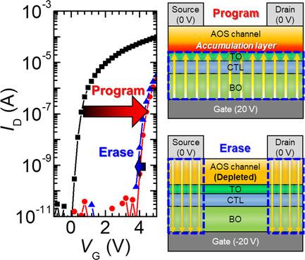
A charge‐trap flash (CTF) device is fabricated using atomic‐layer‐deposited zinc tin oxide (ZTO) as an n‐type amorphous oxide semiconductor (AOS) channel layer and its program/erase characteristics are examined. When a positive voltage of 20 V is applied to the gate electrode, electrons are fluently injected into the adopted SiNx charge trap layer, resulting in a program operation showing a threshold voltage (Vth) shift of 3.7 V. However, even when −20 V is applied for up to 10 s, the trapped electrons are not detrapped. Instead, it is possible to recover Vth to its initial value only by the irradiation of white light. To understand this phenomenon, a ZTO CTF device is modeled using the technology computer‐aided design (TCAD) simulation package. The high hole injection barrier between the source/drain and the ZTO channel prohibits hole injection, which is the cause of the inefficient erasing. It is also confirmed that an AOS CTF with sufficient program and erase speed would be limited by the inherent energy band structure of AOS with its wide bandgap of over 3 eV. An alternative method of using the fringing field effect according to channel length scaling is proposed.
中文翻译:

调查具有非晶氧化物半导体薄膜通道层的电荷陷阱闪存设备难以擦除操作的原因
使用原子层沉积的氧化锌锡(ZTO)作为n型非晶氧化物半导体(AOS)沟道层制造电荷陷阱闪存(CTF)器件,并检查其编程/擦除特性。当向栅电极施加20 V的正电压时,电子被流畅地注入所采用的SiN x电荷陷阱层中,从而导致编程操作显示出3.7 V的阈值电压(V th)漂移。但是,即使-施加20 V电压长达10 s,被俘获的电子不会被俘获。相反,有可能恢复V th只能通过照射白光使其达到初始值。为了理解这种现象,使用技术计算机辅助设计(TCAD)仿真软件包对ZTO CTF设备进行了建模。源极/漏极与ZTO通道之间的高空穴注入势垒会阻止空穴注入,这是导致擦除效率低下的原因。还证实了具有足够的编程和擦除速度的AOS CTF将受到其宽带隙超过3 eV的AOS固有能带结构的限制。提出了一种根据信道长度缩放使用边缘场效应的替代方法。
更新日期:2021-02-09
中文翻译:
调查具有非晶氧化物半导体薄膜通道层的电荷陷阱闪存设备难以擦除操作的原因
使用原子层沉积的氧化锌锡(ZTO)作为n型非晶氧化物半导体(AOS)沟道层制造电荷陷阱闪存(CTF)器件,并检查其编程/擦除特性。当向栅电极施加20 V的正电压时,电子被流畅地注入所采用的SiN x电荷陷阱层中,从而导致编程操作显示出3.7 V的阈值电压(V th)漂移。但是,即使-施加20 V电压长达10 s,被俘获的电子不会被俘获。相反,有可能恢复V th只能通过照射白光使其达到初始值。为了理解这种现象,使用技术计算机辅助设计(TCAD)仿真软件包对ZTO CTF设备进行了建模。源极/漏极与ZTO通道之间的高空穴注入势垒会阻止空穴注入,这是导致擦除效率低下的原因。还证实了具有足够的编程和擦除速度的AOS CTF将受到其宽带隙超过3 eV的AOS固有能带结构的限制。提出了一种根据信道长度缩放使用边缘场效应的替代方法。


 京公网安备 11010802027423号