Micro and Nanostructures ( IF 2.7 ) Pub Date : 2020-12-22 , DOI: 10.1016/j.spmi.2020.106785 Monika P. Joshi , Popatrao N. Bhosale
|
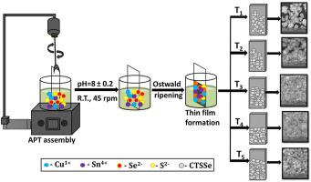
A novel chemical approach is utilized to synthesize Cu2Sn(S,Se)3 (CTSSe) thin films by non-vacuum arrested precipitation technique (APT) via controlled release of ions from complexed solution. Effect of deposition time on the microstructural and optoelectronic properties of CTSSe thin films was studied comprehensively. The optical absorption studies demonstrate a decrease in band gap energy from 1.84 to 1.62 eV as the deposition time increases. Nanocrystalline thin films with improved grain size were illustrated from XRD studies. The FESEM micrographs depict progress in surface microstructure from a bunch of nanospheres to aggregated and densely packed nanospheres. EDS spectrum confirms the stoichiometric formation of Cu2Sn(S,Se)3 thin film. While, the XPS spectrum validates Cu1+, Sn4+, S2-, Se2-valence states of the elements in CTSSe thin film. Furthermore, the photoelectrochemical cell performance of 0.3 % for bare CTSSe thin film was elucidated with cell configuration glass-FTO/CTSSe/(I-/I3-)/graphite without any post deposition treatments. Also, the lowering of charge transfer resistance from EIS measurements corroborates for improved photoconversion efficiency. Finally, synthesis of CTSSe thin films by a simple APT finds a promising approach to fabricate efficient CTSSe photocathode for photovoltaic applications.
中文翻译:
探索通过非真空阻滞沉淀技术合成的沉积时间相关的Cu 2 Sn(S,Se)3薄膜的微结构,光电性能
利用一种新型的化学方法,通过控制复合溶液中离子的释放,通过非真空阻滞沉淀技术(APT)合成Cu 2 Sn(S,Se)3(CTSSe)薄膜。全面研究了沉积时间对CTSSe薄膜微结构和光电性能的影响。光吸收研究表明,随着沉积时间的增加,带隙能量从1.84 eV降低到1.62 eV。XRD研究表明了具有改善的晶粒尺寸的纳米晶体薄膜。FESEM显微照片描述了从一堆纳米球到聚集和密集堆积的纳米球的表面微观结构的进展。EDS光谱证实了Cu 2 Sn(S,Se)3的化学计量形成薄膜。同时,XPS光谱验证了CTSSe薄膜中元素的Cu 1+,Sn 4+,S 2-,Se 2-价态。此外,对于裸CTSSe薄膜的0.3%的光电化学电池的性能与小区配置玻璃FTO / CTSSe /(I阐明- / I 3 - /无需任何后处理沉积石墨)。同样,从EIS测量结果得出的电荷转移电阻的降低也证实了改进的光转换效率。最后,通过简单的APT合成CTSSe薄膜发现了一种有前途的方法来制造用于光伏应用的高效CTSSe光电阴极。


 京公网安备 11010802027423号