当前位置:
X-MOL 学术
›
Phys. Status Solidi A
›
论文详情
Our official English website, www.x-mol.net, welcomes your feedback! (Note: you will need to create a separate account there.)
The Significant Effect of Carbon and Oxygen Contaminants at Pd/p‐GaN Interface on Its Ohmic Contact Characteristics
Physica Status Solidi (A) - Applications and Materials Science ( IF 2 ) Pub Date : 2020-12-11 , DOI: 10.1002/pssa.202000603 Zhengcheng Li 1, 2 , Rong Huang 2 , Xiao Chen 2 , Hu Wang 2 , Boyuan Feng 1, 2 , Gaohang He 2 , Zengli Huang 2 , Fangsen Li 2 , Jianping Liu 2 , Liqun Zhang 2 , Tong Liu 2 , Sunan Ding 1, 2
Physica Status Solidi (A) - Applications and Materials Science ( IF 2 ) Pub Date : 2020-12-11 , DOI: 10.1002/pssa.202000603 Zhengcheng Li 1, 2 , Rong Huang 2 , Xiao Chen 2 , Hu Wang 2 , Boyuan Feng 1, 2 , Gaohang He 2 , Zengli Huang 2 , Fangsen Li 2 , Jianping Liu 2 , Liqun Zhang 2 , Tong Liu 2 , Sunan Ding 1, 2
Affiliation
|
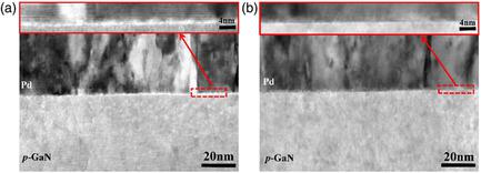
A low‐resistance Ohmic contact of Pd/Pt/Au metallization scheme is formed on a p‐type GaN film grown by metal‐organic chemical vapor deposition (MOCVD). Two samples are prepared to explore the effect of contaminations at the metal and GaN interface on the properties of the Ohmic contact. One directly transfers the fresh GaN film from MOCVD to the metal deposition chamber through an ultrahigh vacuum (UHV) tube, without exposing the GaN surface to air; the other transfers the GaN film from MOCVD to metal deposition through the atmosphere. The results show a lower specific contact resistance (6.2 ± 0.9) × 10−5 Ω cm2 for the directly UHV‐transferred sample than the air‐transferred sample (2.1 ± 0.9) × 10−4 Ω cm2. Once exposed to air, carbonaceous particles and an amorphous oxide layer easily adhere to the p‐type GaN surface, which not only increase the Schottky barrier height but also generate more grain boundaries in the Pd/Pt/Au stacks. The grain boundaries, acting as diffusion channels, make Au atoms diffuse easily into the Pd layer and propagate to the p‐GaN surface layer after annealing. Therefore, the Ohmic contact fabricated in UHV ambience with lower oxygen and carbon contaminations at the interface shows superior characteristics than the samples prepared by the traditional method.
中文翻译:

Pd / p-GaN界面上的碳和氧污染物对其欧姆接触特性的重要影响
在通过金属有机化学气相沉积(MOCVD)生长的ap型GaN膜上形成了Pd / Pt / Au金属化方案的低电阻欧姆接触。准备两个样品,以研究金属和GaN界面处的污染物对欧姆接触特性的影响。一种是通过超高真空(UHV)管将新鲜的GaN膜从MOCVD直接转移到金属沉积室,而又不将GaN表面暴露在空气中。另一层则通过大气将GaN膜从MOCVD转移到金属沉积。结果显示出较低的固有接触电阻(6.2±0.9)×10 -5 Ω厘米2为比空气转印样品(2.1±0.9)×10的直接UHV-转移样品-4 Ω厘米2。一旦暴露在空气中,碳质颗粒和无定形氧化物层很容易粘附到p型GaN表面,这不仅增加了肖特基势垒高度,而且在Pd / Pt / Au堆中产生了更多的晶界。充当扩散通道的晶界使Au原子易于扩散到Pd层中,并在退火后传播到p-GaN表面层。因此,与传统方法制备的样品相比,在UHV环境中制造的欧姆接触在界面处具有较低的氧气和碳污染,具有更好的特性。
更新日期:2021-02-17
中文翻译:
Pd / p-GaN界面上的碳和氧污染物对其欧姆接触特性的重要影响
在通过金属有机化学气相沉积(MOCVD)生长的ap型GaN膜上形成了Pd / Pt / Au金属化方案的低电阻欧姆接触。准备两个样品,以研究金属和GaN界面处的污染物对欧姆接触特性的影响。一种是通过超高真空(UHV)管将新鲜的GaN膜从MOCVD直接转移到金属沉积室,而又不将GaN表面暴露在空气中。另一层则通过大气将GaN膜从MOCVD转移到金属沉积。结果显示出较低的固有接触电阻(6.2±0.9)×10 -5 Ω厘米2为比空气转印样品(2.1±0.9)×10的直接UHV-转移样品-4 Ω厘米2。一旦暴露在空气中,碳质颗粒和无定形氧化物层很容易粘附到p型GaN表面,这不仅增加了肖特基势垒高度,而且在Pd / Pt / Au堆中产生了更多的晶界。充当扩散通道的晶界使Au原子易于扩散到Pd层中,并在退火后传播到p-GaN表面层。因此,与传统方法制备的样品相比,在UHV环境中制造的欧姆接触在界面处具有较低的氧气和碳污染,具有更好的特性。


 京公网安备 11010802027423号