当前位置:
X-MOL 学术
›
Microelectron. Eng.
›
论文详情
Our official English website, www.x-mol.net, welcomes your
feedback! (Note: you will need to create a separate account there.)
Observation of different transport behaviors in a two-dimensional MoTe2 field-effect transistor with engineered gate stack
Microelectronic Engineering ( IF 2.6 ) Pub Date : 2021-01-01 , DOI: 10.1016/j.mee.2020.111497 Yafen Yang , Xinyi Zhu , Kai Zhang , Hao Zhu , Lin Chen , Qingqing Sun
Microelectronic Engineering ( IF 2.6 ) Pub Date : 2021-01-01 , DOI: 10.1016/j.mee.2020.111497 Yafen Yang , Xinyi Zhu , Kai Zhang , Hao Zhu , Lin Chen , Qingqing Sun
|
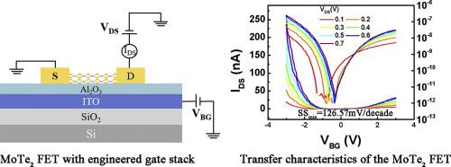
Abstract Back-gate field-effect transistor (FET) fabricated from exfoliated two-dimensional (2D) materials have been widely applied on the electronic device applications of the novel transition metal dichalcogenides (TMDs) since their experimental discovery. Si substrate covered with thick SiO2 dielectric layer is commonly used due to the natural back-gate geometry and good optical contrast which, however, lacks sufficient gate control over the ultra-thin channel because of the thick dielectric. Here, in this work, we report a high-performance back-gate MoTe2 FET fabricated on a novel Al2O3/ITO (indium tin oxide)/SiO2/Si stack substrate. The stack thickness has been carefully designed and engineered to enhance the gate control of the MoTe2 channel while enabling sufficient optical contrast between the substrate and the exfoliated 2D flakes. Unipolar and ambipolar transport behaviors on different substrates have been observed and analyzed. As compared to the conventional 300 nm SiO2/Si substrate, the MoTe2 FET on the engineered gate stack has exhibited higher on/off current ratio with smaller cut-off current and smaller subthreshold slope of 126.57 mV/dec. These results are attractive in building novel logic devices based on the 2D MoTe2 with unipolar and ambipolar behavior broadening the applications in advanced nanoelectronics and optoelectronics systems
中文翻译:

观察具有工程化栅极堆叠的二维 MoTe2 场效应晶体管中的不同传输行为
摘要 由剥离二维 (2D) 材料制成的背栅场效应晶体管 (FET) 自实验发现以来已广泛应用于新型过渡金属二硫属化物 (TMD) 的电子器件应用中。由于自然的背栅几何形状和良好的光学对比度,通常使用覆盖有厚 SiO2 电介质层的 Si 衬底,然而,由于厚电介质,这对超薄沟道缺乏足够的栅极控制。在这里,在这项工作中,我们报告了一种在新型 Al2O3/ITO(氧化铟锡)/SiO2/Si 堆叠基板上制造的高性能背栅 MoTe2 FET。堆叠厚度经过精心设计和设计,以增强 MoTe2 通道的栅极控制,同时在基板和剥离的 2D 薄片之间实现足够的光学对比度。已经观察和分析了不同基材上的单极和双极传输行为。与传统的 300 nm SiO2/Si 衬底相比,工程化栅极堆叠上的 MoTe2 FET 具有更高的开/关电流比,具有更小的截止电流和更小的亚阈值斜率 126.57 mV/dec。这些结果在构建基于具有单极和双极行为的 2D MoTe2 的新型逻辑器件方面具有吸引力,从而拓宽了在先进纳米电子和光电子系统中的应用
更新日期:2021-01-01
中文翻译:
观察具有工程化栅极堆叠的二维 MoTe2 场效应晶体管中的不同传输行为
摘要 由剥离二维 (2D) 材料制成的背栅场效应晶体管 (FET) 自实验发现以来已广泛应用于新型过渡金属二硫属化物 (TMD) 的电子器件应用中。由于自然的背栅几何形状和良好的光学对比度,通常使用覆盖有厚 SiO2 电介质层的 Si 衬底,然而,由于厚电介质,这对超薄沟道缺乏足够的栅极控制。在这里,在这项工作中,我们报告了一种在新型 Al2O3/ITO(氧化铟锡)/SiO2/Si 堆叠基板上制造的高性能背栅 MoTe2 FET。堆叠厚度经过精心设计和设计,以增强 MoTe2 通道的栅极控制,同时在基板和剥离的 2D 薄片之间实现足够的光学对比度。已经观察和分析了不同基材上的单极和双极传输行为。与传统的 300 nm SiO2/Si 衬底相比,工程化栅极堆叠上的 MoTe2 FET 具有更高的开/关电流比,具有更小的截止电流和更小的亚阈值斜率 126.57 mV/dec。这些结果在构建基于具有单极和双极行为的 2D MoTe2 的新型逻辑器件方面具有吸引力,从而拓宽了在先进纳米电子和光电子系统中的应用


 京公网安备 11010802027423号