当前位置:
X-MOL 学术
›
J. Mater. Sci.
›
论文详情
Our official English website, www.x-mol.net, welcomes your
feedback! (Note: you will need to create a separate account there.)
Novel rare earth yttrium doping effect on physical properties of PbS nanostructures: facile synthesis and characterization
Journal of Materials Science ( IF 3.5 ) Pub Date : 2020-11-30 , DOI: 10.1007/s10853-020-05539-w Kamlesh V. Chandekar , T. Alshahrani , A. Ben Gouider Trabelsi , F. H. Alkallas , Mohd. Shkir , S. AlFaify
Journal of Materials Science ( IF 3.5 ) Pub Date : 2020-11-30 , DOI: 10.1007/s10853-020-05539-w Kamlesh V. Chandekar , T. Alshahrani , A. Ben Gouider Trabelsi , F. H. Alkallas , Mohd. Shkir , S. AlFaify
|
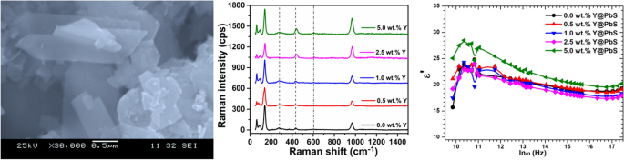
The dielectric properties of pure and yttrium-doped PbS nanoparticles synthesized by the coprecipitation chemical synthesis route have been studied by several characterizations. X-ray diffraction patterns of samples were employed to estimate the crystallite sizes and intrinsic microstrains using Williamson–Hall (W–H) plot analysis. The crystallite size and intrinsic macrostrain values were evaluated in the range of 13.7–15.9 nm and 1.09 × 10⁻³–1.72 × 10⁻³, respectively, using W–H plots. The formation of nanoparticles, nanoflakes, sponge, and nanosheets were seen via scanning electron microscope (SEM). Energy dispersive spectroscopy (EDS) of 5.0 wt% confirms the Y: PbS sample elements' chemical composition and stoichiometry. The optical band gaps increase in the range of (0.93–1.17 eV) with an increase in the dislocation density. The higher values of dielectric constant (23.6–28.0), dielectric loss (37.6–176.8), loss tangent (2.7–8.6), and electrical conductivity [ 10.2 to ( 11.7) S/m] have been reported at the lower frequency. The highest electrical conductivity values were obtained in the range of [ 4.71 to ( 4.81) S/m] for as-prepared samples. The greater capacitance and impedance values were found at 3 kHz and decrease with increasing the frequency up to 10 MHz. The current–voltage characteristic curves of undoped and Y: PbS NPs were performed under biased voltage. The space charge current density was noticed in the range of (8.7 × 10⁻⁴–4.2 × 10⁻⁴ amp/cm2) at 1.0, 2.5, and 5.0 wt% of Y: PbS samples. The enhancement in the optical band gap and dielectric and electric properties on yttrium doping in PbS compared to pristine PbS NPs makes them suitable for optoelectronic applications.
中文翻译:

新型稀土钇掺杂对 PbS 纳米结构物理性质的影响:简便的合成和表征
通过多种表征研究了通过共沉淀化学合成途径合成的纯和掺钇 PbS 纳米粒子的介电特性。使用威廉姆森-霍尔 (W-H) 图分析,采用样品的 X 射线衍射图来估计微晶尺寸和固有微应变。使用 W-H 图分别在 13.7-15.9 nm 和 1.09 × 10⁻³-1.72 × 10⁻³ 范围内评估微晶尺寸和固有宏观应变值。通过扫描电子显微镜 (SEM) 观察到纳米颗粒、纳米薄片、海绵和纳米片的形成。5.0 wt% 的能量色散光谱 (EDS) 证实了 Y:PbS 样品元素的化学成分和化学计量。随着位错密度的增加,光学带隙在(0.93-1.17 eV)范围内增加。较高的介电常数 (23.6–28.0)、介电损耗 (37.6–176.8)、损耗角正切 (2.7–8.6) 和电导率 [10.2 至 (11.7) S/m] 的较高值已在较低频率下报道。对于所制备的样品,在 [4.71 至 (4.81) S/m] 范围内获得了最高电导率值。在 3 kHz 处发现了更大的电容和阻抗值,并且随着频率增加到 10 MHz 而减小。未掺杂和 Y:PbS NPs 的电流-电压特性曲线在偏置电压下进行。在 Y: PbS 样品的 1.0、2.5 和 5.0 wt% 的范围内观察到空间电荷电流密度 (8.7 × 10⁻⁴–4.2 × 10⁻⁴ amp/cm2)。
更新日期:2020-11-30
中文翻译:
新型稀土钇掺杂对 PbS 纳米结构物理性质的影响:简便的合成和表征
通过多种表征研究了通过共沉淀化学合成途径合成的纯和掺钇 PbS 纳米粒子的介电特性。使用威廉姆森-霍尔 (W-H) 图分析,采用样品的 X 射线衍射图来估计微晶尺寸和固有微应变。使用 W-H 图分别在 13.7-15.9 nm 和 1.09 × 10⁻³-1.72 × 10⁻³ 范围内评估微晶尺寸和固有宏观应变值。通过扫描电子显微镜 (SEM) 观察到纳米颗粒、纳米薄片、海绵和纳米片的形成。5.0 wt% 的能量色散光谱 (EDS) 证实了 Y:PbS 样品元素的化学成分和化学计量。随着位错密度的增加,光学带隙在(0.93-1.17 eV)范围内增加。较高的介电常数 (23.6–28.0)、介电损耗 (37.6–176.8)、损耗角正切 (2.7–8.6) 和电导率 [10.2 至 (11.7) S/m] 的较高值已在较低频率下报道。对于所制备的样品,在 [4.71 至 (4.81) S/m] 范围内获得了最高电导率值。在 3 kHz 处发现了更大的电容和阻抗值,并且随着频率增加到 10 MHz 而减小。未掺杂和 Y:PbS NPs 的电流-电压特性曲线在偏置电压下进行。在 Y: PbS 样品的 1.0、2.5 和 5.0 wt% 的范围内观察到空间电荷电流密度 (8.7 × 10⁻⁴–4.2 × 10⁻⁴ amp/cm2)。


 京公网安备 11010802027423号