当前位置:
X-MOL 学术
›
Mater. Today
›
论文详情
Our official English website, www.x-mol.net, welcomes your
feedback! (Note: you will need to create a separate account there.)
Laser writing of electronic circuitry in thin film molybdenum disulfide: A transformative manufacturing approach
Materials Today ( IF 21.1 ) Pub Date : 2020-12-01 , DOI: 10.1016/j.mattod.2020.09.036 Drake Austin , Kimberly Gliebe , Christopher Muratore , Bryce Boyer , Timothy S. Fisher , Lucas K. Beagle , Anna Benton , Paige Look , David Moore , Emilie Ringe , Benjamin Treml , Ali Jawaid , Richard Vaia , W. Joshua Kennedy , Philip Buskohl , Nicholas R. Glavin
Materials Today ( IF 21.1 ) Pub Date : 2020-12-01 , DOI: 10.1016/j.mattod.2020.09.036 Drake Austin , Kimberly Gliebe , Christopher Muratore , Bryce Boyer , Timothy S. Fisher , Lucas K. Beagle , Anna Benton , Paige Look , David Moore , Emilie Ringe , Benjamin Treml , Ali Jawaid , Richard Vaia , W. Joshua Kennedy , Philip Buskohl , Nicholas R. Glavin
|
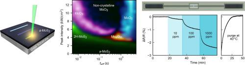
Abstract Electronic circuits, the backbone of modern electronic devices, require precise integration of conducting, insulating, and semiconducting materials in two- and three-dimensional space to control the flow of electric current. Alternative strategies to pattern these materials outside of a cleanroom environment, such as additive manufacturing, have enabled rapid prototyping and eliminated design constraints imposed by traditional fabrication. In this work, a transformative manufacturing approach using laser processing is implemented to directly realize conducting, insulating, and semiconducting phases within an amorphous molybdenum disulfide thin film precursor. This is achieved by varying the incident visible (514 nm) laser intensity and raster-scanning the thin film a-MoS2 sample (900 nm thick) at different speeds for micro-scale control of the crystallization and reaction kinetics. The overall result is the transformation of select regions of the a-MoS2 film into MoO2, MoO3, and 2H-MoS2 phases, exhibiting conducting, insulating, and semiconducting properties, respectively. A mechanism for this precursor transformation based on crystallization and oxidation is developed using a thermal model paired with a description of the reaction kinetics. Finally, by engineering the architecture of the three crystalline phases, electrical devices such as a resistor, capacitor, and chemical sensor were laser-written directly within the precursor film, representing an entirely transformative manufacturing approach for the fabrication of electronic circuitry.
中文翻译:

二硫化钼薄膜电子电路的激光写入:一种变革性的制造方法
摘要 电子电路是现代电子设备的支柱,需要在二维和三维空间中精确集成导电、绝缘和半导体材料来控制电流的流动。在洁净室环境之外对这些材料进行图案化的替代策略,例如增材制造,已经实现了快速原型制作并消除了传统制造所施加的设计限制。在这项工作中,实施了一种使用激光加工的变革性制造方法,以在非晶二硫化钼薄膜前驱体中直接实现导电、绝缘和半导体相。这是通过改变入射可见光 (514 nm) 激光强度和光栅扫描薄膜 a-MoS2 样品(900 nm 厚)以不同速度实现的,以对结晶和反应动力学进行微尺度控制。总体结果是 a-MoS2 膜的选定区域转变为 MoO2、MoO3 和 2H-MoS2 相,分别表现出导电、绝缘和半导体特性。这种基于结晶和氧化的前体转化机制是使用热模型与反应动力学描述相结合的。最后,通过设计三个晶相的结构,将电阻器、电容器和化学传感器等电子器件直接激光写入前体膜中,
更新日期:2020-12-01
中文翻译:
二硫化钼薄膜电子电路的激光写入:一种变革性的制造方法
摘要 电子电路是现代电子设备的支柱,需要在二维和三维空间中精确集成导电、绝缘和半导体材料来控制电流的流动。在洁净室环境之外对这些材料进行图案化的替代策略,例如增材制造,已经实现了快速原型制作并消除了传统制造所施加的设计限制。在这项工作中,实施了一种使用激光加工的变革性制造方法,以在非晶二硫化钼薄膜前驱体中直接实现导电、绝缘和半导体相。这是通过改变入射可见光 (514 nm) 激光强度和光栅扫描薄膜 a-MoS2 样品(900 nm 厚)以不同速度实现的,以对结晶和反应动力学进行微尺度控制。总体结果是 a-MoS2 膜的选定区域转变为 MoO2、MoO3 和 2H-MoS2 相,分别表现出导电、绝缘和半导体特性。这种基于结晶和氧化的前体转化机制是使用热模型与反应动力学描述相结合的。最后,通过设计三个晶相的结构,将电阻器、电容器和化学传感器等电子器件直接激光写入前体膜中,


 京公网安备 11010802027423号