当前位置:
X-MOL 学术
›
Adv. Electron. Mater.
›
论文详情
Our official English website, www.x-mol.net, welcomes your
feedback! (Note: you will need to create a separate account there.)
Characterization of a 2D Electron Gas at the Interface of Atomic‐Layer Deposited Al2O3/ZnO Thin Films for a Field‐Effect Transistor
Advanced Electronic Materials ( IF 5.3 ) Pub Date : 2020-12-04 , DOI: 10.1002/aelm.202000876 Hyun Jae Lee 1 , Taehwan Moon 1, 2 , Seung Dam Hyun 1 , Sukin Kang 1 , Cheol Seong Hwang 1
Advanced Electronic Materials ( IF 5.3 ) Pub Date : 2020-12-04 , DOI: 10.1002/aelm.202000876 Hyun Jae Lee 1 , Taehwan Moon 1, 2 , Seung Dam Hyun 1 , Sukin Kang 1 , Cheol Seong Hwang 1
Affiliation
|
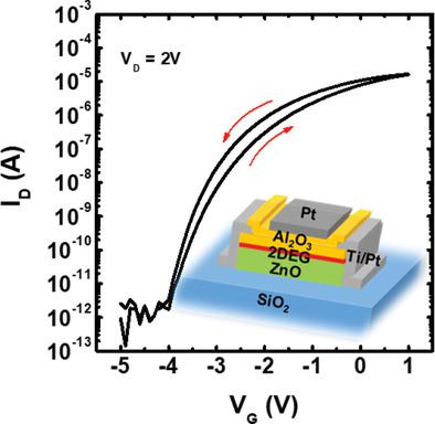
The 2D electron gas (2DEG) phenomenon that occurs at the amorphous thin film hetero‐oxide interface attracts great attention since it can avoid the use of a single‐crystal oxide substrate. In this study, the analysis of 2DEG at the interface of amorphous‐Al2O3 (a‐AO)/ZnO is conducted using ZnO as the bottom substrate, where both the oxide films are grown by atomic layer deposition. Having used Al(CH3)3 as the Al‐precursor for the a‐AO film growth on the previously grown ZnO film, its strong reducing power induces the 2DEG formation at the interface. As a result of the Hall measurement, the 2DEG at the a‐AO/ZnO interface shows sheet resistance of 2.7 × 10⁴ Ω ▫−1 and Hall mobility of 8.4 cm2 V−1 s−1. Using angle‐resolved X‐ray photoelectron spectroscopy, the thickness of the 2DEG layer is calculated as 0.62 nm, which is ≈120% of the c‐axis of the wurtzite ZnO unit cell. The field‐effect transistor fabricated exhibits a threshold voltage of −2.4 V, sub‐threshold swing of 0.33 V dec−1, and on/off ratio of 9.4 × 10⁶, which significantly outperforms similar devices from previous works. The outstanding operation of 2DEG at the interface of AO/ZnO as a channel presents a possibility for application to a 2D‐based integrated circuit.
中文翻译:

场效应晶体管在原子层沉积的Al2O3 / ZnO薄膜界面处的二维电子气的表征
由于可以避免使用单晶氧化物衬底,因此在非晶薄膜杂氧化物界面上发生的2D电子气(2DEG)现象备受关注。在这项研究中,使用ZnO作为底部衬底对非晶-Al 2 O 3(a- AO)/ ZnO界面处的2DEG进行分析,两个氧化物膜均通过原子层沉积生长。在先前生长的ZnO薄膜上使用Al(CH 3)3作为a - AO薄膜生长的Al前驱物后,其强大的还原能力会在界面处诱发2DEG的形成。霍尔测量的结果是,a- AO / ZnO界面上的2DEG的薄层电阻为2.7×10⁴ Ω▫ -1和霍尔迁移率的8.4厘米2 V -1 小号-1。使用角分辨X射线光电子能谱,计算得出2DEG层的厚度为0.62 nm,约为纤锌矿型ZnO晶胞c轴的120%。制作的场效应晶体管的阈值电压为-2.4 V,亚阈值摆幅为0.33 V dec -1,开/关比为9.4×10 6,明显优于以前的工作。2DEG在AO / ZnO接口作为通道的出色操作为应用到基于2D的集成电路提供了可能性。
更新日期:2021-01-14
中文翻译:
场效应晶体管在原子层沉积的Al2O3 / ZnO薄膜界面处的二维电子气的表征
由于可以避免使用单晶氧化物衬底,因此在非晶薄膜杂氧化物界面上发生的2D电子气(2DEG)现象备受关注。在这项研究中,使用ZnO作为底部衬底对非晶-Al 2 O 3(a- AO)/ ZnO界面处的2DEG进行分析,两个氧化物膜均通过原子层沉积生长。在先前生长的ZnO薄膜上使用Al(CH 3)3作为a - AO薄膜生长的Al前驱物后,其强大的还原能力会在界面处诱发2DEG的形成。霍尔测量的结果是,a- AO / ZnO界面上的2DEG的薄层电阻为2.7×10⁴ Ω▫ -1和霍尔迁移率的8.4厘米2 V -1 小号-1。使用角分辨X射线光电子能谱,计算得出2DEG层的厚度为0.62 nm,约为纤锌矿型ZnO晶胞c轴的120%。制作的场效应晶体管的阈值电压为-2.4 V,亚阈值摆幅为0.33 V dec -1,开/关比为9.4×10 6,明显优于以前的工作。2DEG在AO / ZnO接口作为通道的出色操作为应用到基于2D的集成电路提供了可能性。


 京公网安备 11010802027423号