当前位置:
X-MOL 学术
›
Microelectron. Eng.
›
论文详情
Our official English website, www.x-mol.net, welcomes your feedback! (Note: you will need to create a separate account there.)
A novel self-aligned double patterning integrated with Ga+ focused ion beam milling for silicon nanowire definition
Microelectronic Engineering ( IF 2.3 ) Pub Date : 2021-01-01 , DOI: 10.1016/j.mee.2020.111493 Andressa Macedo Rosa , Alessandra Leonhardt , Laís Oliveira de Souza , Lucas Petersen Barbosa Lima , Marcos Vinicius Puydinger dos Santos , Leandro Tiago Manera , José Alexandre Diniz
Microelectronic Engineering ( IF 2.3 ) Pub Date : 2021-01-01 , DOI: 10.1016/j.mee.2020.111493 Andressa Macedo Rosa , Alessandra Leonhardt , Laís Oliveira de Souza , Lucas Petersen Barbosa Lima , Marcos Vinicius Puydinger dos Santos , Leandro Tiago Manera , José Alexandre Diniz
|
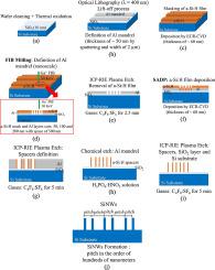
Abstract Self-aligned double (SADP) or quadruple (SAQP) patternings have been used to obtain sub-resolution lithographies (sub-10 nm). For this purpose, usually, these patternings are integrated with 193 nm immersion (193iL), extreme ultra-violet (EUVL) and electron beam (EBL) lithographies. In this work, SADPs are integrated with Ga+ Focused Ion Beam (FIB) milling, which is a novel alternative to traditional 193iL, EUVL and EBL, mainly for prototyping of nanodevices. Furthermore, the FIB milling is a maskless process, thus being more flexible than EBL and cheaper than EUVL. The FIB milling was carried out on the a-Si:H/Al (deposited on Si substrate) to pattern the parallel Al nanowires (AlNWs), which are used as mandrel in our SADP. The a-Si:H layer, used as spacer in our SADP, also is an effective barrier against the Ga+ ion bombardment directly on Al surface, avoiding damages on the AlNW mandrel. Thus, after FIB milling, SADP and plasma etch steps, Silicon Nano-Wires (SiNWs), with dimensions (extracted by Scaning Electron Microscopy (SEM)) of fin width and pitch of 35 nm and 170 nm, respectively, were obtained. This is an excellent result, similar to obtained by SADP methods integrated with traditional lithographies. Therefore, our SADP with FIB milling is a flexible alternative to obtain SiNWs for 3D nanostructure technologies prototypes. Furthermore, a last important result, extracted from energy dispersive x-ray spectroscopy (EDS) spectrum, is the Ga peak absence, indicating that no trace of gallium (for an EDS detection limit of 1%) could be detected into SiNWs. This result agrees the TRIM (Transport and Range of Ions in Matter) simulation of gallium ion implantation in a-Si:H/Al structure.
中文翻译:

一种用于硅纳米线定义的新型自对准双图案与 Ga+ 聚焦离子束铣削集成
摘要 自对准双 (SADP) 或四重 (SAQP) 图案化已被用于获得亚分辨率光刻 (sub-10 nm)。为此,通常将这些图案与 193 nm 浸没 (193iL)、极紫外 (EUVL) 和电子束 (EBL) 光刻相结合。在这项工作中,SADP 与 Ga+ 聚焦离子束 (FIB) 铣削相结合,这是传统 193iL、EUVL 和 EBL 的新型替代品,主要用于纳米器件的原型制作。此外,FIB 铣削是一种无掩模工艺,因此比 EBL 更灵活且比 EUVL 便宜。FIB 铣削在 a-Si:H/Al(沉积在 Si 衬底上)上进行以图案化平行的 Al 纳米线(AlNWs),其在我们的 SADP 中用作心轴。a-Si:H 层,在我们的 SADP 中用作隔离物,也是防止 Ga+ 离子直接轰击 Al 表面的有效屏障,避免损坏 AlNW 心轴。因此,在 FIB 铣削、SADP 和等离子体蚀刻步骤之后,获得了尺寸(通过扫描电子显微镜(SEM)提取)的鳍片宽度和间距分别为 35 nm 和 170 nm 的硅纳米线(SiNW)。这是一个很好的结果,类似于通过与传统光刻集成的 SADP 方法获得的结果。因此,我们的带有 FIB 铣削的 SADP 是获得用于 3D 纳米结构技术原型的 SiNW 的灵活替代方案。此外,从能量色散 X 射线光谱 (EDS) 光谱中提取的最后一个重要结果是 Ga 峰缺失,表明在 SiNW 中没有检测到痕量镓(EDS 检测限为 1%)。
更新日期:2021-01-01
中文翻译:
一种用于硅纳米线定义的新型自对准双图案与 Ga+ 聚焦离子束铣削集成
摘要 自对准双 (SADP) 或四重 (SAQP) 图案化已被用于获得亚分辨率光刻 (sub-10 nm)。为此,通常将这些图案与 193 nm 浸没 (193iL)、极紫外 (EUVL) 和电子束 (EBL) 光刻相结合。在这项工作中,SADP 与 Ga+ 聚焦离子束 (FIB) 铣削相结合,这是传统 193iL、EUVL 和 EBL 的新型替代品,主要用于纳米器件的原型制作。此外,FIB 铣削是一种无掩模工艺,因此比 EBL 更灵活且比 EUVL 便宜。FIB 铣削在 a-Si:H/Al(沉积在 Si 衬底上)上进行以图案化平行的 Al 纳米线(AlNWs),其在我们的 SADP 中用作心轴。a-Si:H 层,在我们的 SADP 中用作隔离物,也是防止 Ga+ 离子直接轰击 Al 表面的有效屏障,避免损坏 AlNW 心轴。因此,在 FIB 铣削、SADP 和等离子体蚀刻步骤之后,获得了尺寸(通过扫描电子显微镜(SEM)提取)的鳍片宽度和间距分别为 35 nm 和 170 nm 的硅纳米线(SiNW)。这是一个很好的结果,类似于通过与传统光刻集成的 SADP 方法获得的结果。因此,我们的带有 FIB 铣削的 SADP 是获得用于 3D 纳米结构技术原型的 SiNW 的灵活替代方案。此外,从能量色散 X 射线光谱 (EDS) 光谱中提取的最后一个重要结果是 Ga 峰缺失,表明在 SiNW 中没有检测到痕量镓(EDS 检测限为 1%)。


 京公网安备 11010802027423号