当前位置:
X-MOL 学术
›
Angew. Chem. Int. Ed.
›
论文详情
Our official English website, www.x-mol.net, welcomes your
feedback! (Note: you will need to create a separate account there.)
Ultrathin Two‐Dimensional Nanostructures: Surface Defects for Morphology‐Driven Enhanced Semiconductor SERS
Angewandte Chemie International Edition ( IF 16.1 ) Pub Date : 2020-11-30 , DOI: 10.1002/anie.202015306 Ge Song 1, 2 , Wenbin Gong 3 , Shan Cong 1, 2, 4, 5 , Zhigang Zhao 1, 2, 4, 5
Angewandte Chemie International Edition ( IF 16.1 ) Pub Date : 2020-11-30 , DOI: 10.1002/anie.202015306 Ge Song 1, 2 , Wenbin Gong 3 , Shan Cong 1, 2, 4, 5 , Zhigang Zhao 1, 2, 4, 5
Affiliation
|
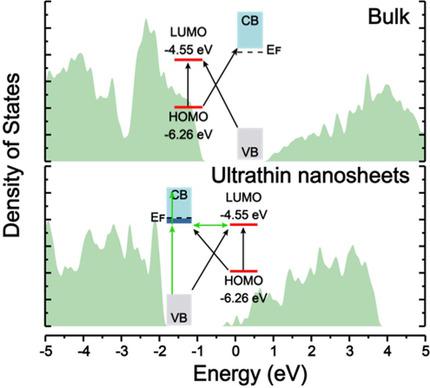
Two‐dimensional (2D) semiconductors have recently become attractive candidate substrates for surface‐enhanced Raman spectroscopy, exhibiting good semiconductor‐based SERS sensing for a wider variety of application scenarios. However, the underlying mechanism remains unclear. Herein, we propose that surface defects play a vital role in the magnification of the SERS performances of 2D semiconductors. As a prototype material, ultrathin WO3 nanosheets is used to demonstrate that surface defect sites and the resulting increased charge‐carrier density can induce strong charge‐transfer interactions at the substrate‐molecule interface, thereby improving the sensitivity of the SERS substrate by 100 times with high reproducibility. Further work with other metal oxides suggests the reduced dimension of 2D materials can be advantageous in promoting SERS sensing for multiple probe molecules.
中文翻译:

超薄二维纳米结构:形态学驱动的增强型半导体SERS的表面缺陷
二维(2D)半导体最近已成为表面增强拉曼光谱的有吸引力的候选衬底,在许多应用场合中都表现出良好的基于半导体的SERS传感。但是,其潜在机制仍不清楚。本文中,我们提出表面缺陷在2D半导体的SERS性能放大中起着至关重要的作用。作为原型材料,超薄WO 3纳米片用于证明表面缺陷位点和由此产生的电荷载流子密度增加可以在底物-分子界面上引起强烈的电荷转移相互作用,从而以高重现性将SERS底物的灵敏度提高了100倍。与其他金属氧化物的进一步研究表明,减小二维材料的尺寸可能有利于促进对多个探针分子的SERS传感。
更新日期:2020-11-30
中文翻译:
超薄二维纳米结构:形态学驱动的增强型半导体SERS的表面缺陷
二维(2D)半导体最近已成为表面增强拉曼光谱的有吸引力的候选衬底,在许多应用场合中都表现出良好的基于半导体的SERS传感。但是,其潜在机制仍不清楚。本文中,我们提出表面缺陷在2D半导体的SERS性能放大中起着至关重要的作用。作为原型材料,超薄WO 3纳米片用于证明表面缺陷位点和由此产生的电荷载流子密度增加可以在底物-分子界面上引起强烈的电荷转移相互作用,从而以高重现性将SERS底物的灵敏度提高了100倍。与其他金属氧化物的进一步研究表明,减小二维材料的尺寸可能有利于促进对多个探针分子的SERS传感。


 京公网安备 11010802027423号