当前位置:
X-MOL 学术
›
Diam. Relat. Mater.
›
论文详情
Our official English website, www.x-mol.net, welcomes your feedback! (Note: you will need to create a separate account there.)
Fabrication of high-quality GaAs/diamond heterointerface for thermal management applications
Diamond and Related Materials ( IF 4.1 ) Pub Date : 2021-01-01 , DOI: 10.1016/j.diamond.2020.108207 Jianbo Liang , Yuji Nakamura , Tianzhuo Zhan , Yutaka Ohno , Yasuo Shimizu , Kazu Katayama , Takanobu Watanabe , Hideto Yoshida , Yasuyoshi Nagai , Hongxing Wang , Makoto Kasu , Naoteru Shigekawa
Diamond and Related Materials ( IF 4.1 ) Pub Date : 2021-01-01 , DOI: 10.1016/j.diamond.2020.108207 Jianbo Liang , Yuji Nakamura , Tianzhuo Zhan , Yutaka Ohno , Yasuo Shimizu , Kazu Katayama , Takanobu Watanabe , Hideto Yoshida , Yasuyoshi Nagai , Hongxing Wang , Makoto Kasu , Naoteru Shigekawa
|
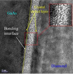
Abstract The direct integrating of GaAs and diamond is achieved at room temperature via a surface activated bonding method. An ultrathin crystal defect layer composed of GaAs and diamond was formed at the bonding interface. The thickness of the GaAs and diamond crystal defect layers was determined to be 0.4 and 1.6 nm, respectively. After annealing at 400 °C, no changes were observed in the thickness of the crystal defect layer and the interfacial structure. The thermal characterization of the transmission line model (TLM) patterns formed on the GaAs layer bonded to diamond and sapphire substrates is demonstrated. The thermal resistance of the GaAs TLM patterns formed on the diamond and sapphire substrates was determined to be 6 and 34.9 K/W, respectively. The GaAs TLM patterns formed on the diamond showed an excellent heat dissipation property due to the high thermal conductivity of diamond.
中文翻译:

用于热管理应用的高质量 GaAs/金刚石异质界面的制造
摘要 通过表面活化键合方法,在室温下实现了 GaAs 和金刚石的直接集成。在结合界面形成由GaAs和金刚石组成的超薄晶体缺陷层。GaAs 和金刚石晶体缺陷层的厚度分别确定为 0.4 和 1.6 nm。400℃退火后,晶体缺陷层厚度和界面结构均未见变化。演示了在与金刚石和蓝宝石衬底结合的 GaAs 层上形成的传输线模型 (TLM) 图案的热特性。在金刚石和蓝宝石衬底上形成的 GaAs TLM 图案的热阻分别确定为 6 和 34.9 K/W。
更新日期:2021-01-01
中文翻译:
用于热管理应用的高质量 GaAs/金刚石异质界面的制造
摘要 通过表面活化键合方法,在室温下实现了 GaAs 和金刚石的直接集成。在结合界面形成由GaAs和金刚石组成的超薄晶体缺陷层。GaAs 和金刚石晶体缺陷层的厚度分别确定为 0.4 和 1.6 nm。400℃退火后,晶体缺陷层厚度和界面结构均未见变化。演示了在与金刚石和蓝宝石衬底结合的 GaAs 层上形成的传输线模型 (TLM) 图案的热特性。在金刚石和蓝宝石衬底上形成的 GaAs TLM 图案的热阻分别确定为 6 和 34.9 K/W。


 京公网安备 11010802027423号