当前位置:
X-MOL 学术
›
Prog. Photovoltaics
›
论文详情
Our official English website, www.x-mol.net, welcomes your
feedback! (Note: you will need to create a separate account there.)
Surface preparation for 10% efficient CZTSe solar cells
Progress in Photovoltaics ( IF 8.0 ) Pub Date : 2020-11-26 , DOI: 10.1002/pip.3356 Louis Grenet 1 , Fabrice Emieux 1 , Léo Choubrac 2 , José A. Márquez 2 , Eric De Vito 1 , Frédéric Roux 1 , Thomas Unold 2
Progress in Photovoltaics ( IF 8.0 ) Pub Date : 2020-11-26 , DOI: 10.1002/pip.3356 Louis Grenet 1 , Fabrice Emieux 1 , Léo Choubrac 2 , José A. Márquez 2 , Eric De Vito 1 , Frédéric Roux 1 , Thomas Unold 2
Affiliation
|
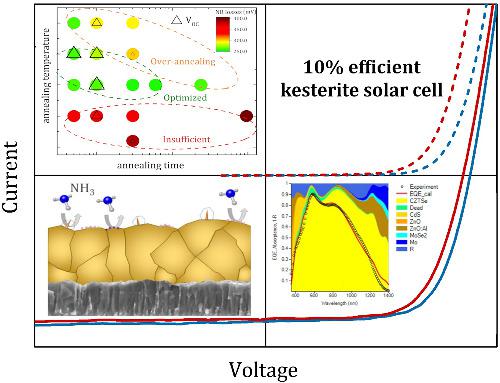
Kesterite‐based solar cells suffer from a large open‐circuit voltage deficit, which largely arises from carrier recombination at the buffer interface. In this study, we compare two strategies to passivate the absorber surface in order to fabricate devices with power conversion efficiency higher than 10% and an open‐circuit voltage deficit as low as 306 mV. These two strategies consist of annealing in air or performing a chemical etching of the absorbers before buffer deposition. They lead similarly to a significant reduction of the interface recombination but as well to a shortening of the minority carrier diffusion length from 1 μm to less than 500 nm. This latter effect limits the short‐circuit current and fill factor of the devices but is largely compensated by the open‐circuit voltage gain of more than 100 mV. For the absorber air annealing, which is the simplest solution to implement, absolute photoluminescence measurements reveal that the voltage gain is directly linked to a drop in the nonradiative losses in the absorber and to a small reduction of the band tailing. It is demonstrated that the removal of detrimental secondary phases at the surface of the absorber due to oxidation at elevated temperature and etching in the basic CdS solution is responsible for these improved opto‐electronic properties. On the contrary, the apparent Cu‐depletion observed after air annealing is totally recovered after the chemical bath and cannot be responsible for the improved performances.
中文翻译:

10%高效CZTSe太阳能电池的表面处理
基于Kesterite的太阳能电池存在很大的开路电压不足,这主要是由于缓冲液界面处的载流子复合所致。在这项研究中,我们比较了两种钝化吸收器表面的策略,以制造功率转换效率高于10%且开路电压赤字低至306 mV的器件。这两种策略包括在空气中退火或在缓冲液沉积之前对吸收体进行化学蚀刻。它们相似地导致界面重组的显着减少,但也导致少数载流子扩散长度从1μm缩短到小于500 nm。后一种效应限制了器件的短路电流和填充因数,但是开路电压增益超过100 mV可以在很大程度上补偿该效应。对于吸收器空气退火,这是最简单的实现方法,绝对光致发光测量表明,电压增益与吸收器中非辐射损耗的下降直接相关,并且与带拖尾的减小有直接关系。事实证明,由于高温下的氧化和在碱性CdS溶液中的蚀刻,吸收剂表面有害的次级相的去除是这些改善的光电性能的原因。相反,在空气退火后观察到的表观的铜耗竭在化学浴后被完全恢复,不能为性能的改善负责。绝对光致发光测量表明,电压增益与吸收体中非辐射损耗的下降直接相关,并且与谱带拖尾的减小程度直接相关。事实证明,由于高温下的氧化和在碱性CdS溶液中的蚀刻,吸收剂表面有害的次级相的去除是这些改善的光电性能的原因。相反,在空气退火后观察到的表观的铜耗竭在化学浴后被完全恢复,不能对性能的改善负责。绝对光致发光测量表明,电压增益直接与吸收体中非辐射损耗的下降以及带拖尾的小幅减少有关。事实证明,由于高温下的氧化和在碱性CdS溶液中的蚀刻,吸收剂表面有害的次级相的去除是这些改善的光电性能的原因。相反,在空气退火后观察到的表观的铜耗竭在化学浴后被完全恢复,不能对性能的改善负责。
更新日期:2021-01-29
中文翻译:
10%高效CZTSe太阳能电池的表面处理
基于Kesterite的太阳能电池存在很大的开路电压不足,这主要是由于缓冲液界面处的载流子复合所致。在这项研究中,我们比较了两种钝化吸收器表面的策略,以制造功率转换效率高于10%且开路电压赤字低至306 mV的器件。这两种策略包括在空气中退火或在缓冲液沉积之前对吸收体进行化学蚀刻。它们相似地导致界面重组的显着减少,但也导致少数载流子扩散长度从1μm缩短到小于500 nm。后一种效应限制了器件的短路电流和填充因数,但是开路电压增益超过100 mV可以在很大程度上补偿该效应。对于吸收器空气退火,这是最简单的实现方法,绝对光致发光测量表明,电压增益与吸收器中非辐射损耗的下降直接相关,并且与带拖尾的减小有直接关系。事实证明,由于高温下的氧化和在碱性CdS溶液中的蚀刻,吸收剂表面有害的次级相的去除是这些改善的光电性能的原因。相反,在空气退火后观察到的表观的铜耗竭在化学浴后被完全恢复,不能为性能的改善负责。绝对光致发光测量表明,电压增益与吸收体中非辐射损耗的下降直接相关,并且与谱带拖尾的减小程度直接相关。事实证明,由于高温下的氧化和在碱性CdS溶液中的蚀刻,吸收剂表面有害的次级相的去除是这些改善的光电性能的原因。相反,在空气退火后观察到的表观的铜耗竭在化学浴后被完全恢复,不能对性能的改善负责。绝对光致发光测量表明,电压增益直接与吸收体中非辐射损耗的下降以及带拖尾的小幅减少有关。事实证明,由于高温下的氧化和在碱性CdS溶液中的蚀刻,吸收剂表面有害的次级相的去除是这些改善的光电性能的原因。相反,在空气退火后观察到的表观的铜耗竭在化学浴后被完全恢复,不能对性能的改善负责。


 京公网安备 11010802027423号