Sensors and Actuators A: Physical ( IF 4.1 ) Pub Date : 2020-11-26 , DOI: 10.1016/j.sna.2020.112449 S. Demirezen , H.G. Çetinkaya , M. Kara , F. Yakuphanoğlu , Ş. Altındal
|
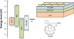
In this study, metal-oxide (NiO:ZnO) nanocomposites mixed with different weight-percentages (2, 10, 20 % NiO) content were coated on the p-Si wafer via spin-coating method. The optical and electrical features of the Al/(PCBM/NiO:ZnO)/p-Si structures/diodes were investigated and compared via current-voltage/time (I–V/t) and capacitance/conductance-voltage-frequency (C/G–V-f) characteristics in dark and various illumination intensities (20, 40, 60, 80, 100 mW/cm2) at room temperature. Main electrical parameters of them such as ideality factor (n), barrier height (Φb), rectification ratio (RR = IF/IR) and series resistance (Rs) were calculated for each percentage (2, 10, and 20 % NiO). Experimental results show that the best percentages of NiO is 20 % in respect of high value of RR and low Rs, but the value of n increases with increasing in percentages. The transient photocurrent increases with increasing illumination level. The slope (m) of the double-logarithmic Iph-P plots were found as 0.67, 0.87 and 0.82, respectively, and these slopes confirmed that these nanocomposites exhibit photoconduction behaviour and hence Al/(PCBM/NiO:ZnO)/p-Si structure can be used a photo device/sensor. The observed changes in the I with illumination, C and G with frequency are the results of interface states (Nss) located at (PCBM/NiO:ZnO)/p-Si interface and so reorder and restructure of them under illumination, bias voltage, and frequency.
中文翻译:
Al /(PCBM / NiO:ZnO)/ p-Si纳米复合结构的合成,电学和光敏特性
在这项研究中,通过旋涂法将混合了不同重量百分比(2%,10%,20%NiO)含量的金属氧化物(NiO:ZnO)纳米复合材料涂覆在p-Si晶片上。研究了Al /(PCBM / NiO:ZnO)/ p-Si结构/二极管的光学和电学特性,并通过电流-电压/时间(IV-t)和电容/电导-电压-频率(C / G–Vf)特性,以及室温下各种光照强度(20、40、60、80、100 mW / cm 2)。它们中的主要的电气参数,例如理想因子(n)时,势垒高度(Φ b),整流比(RR = I ˚F / I - [R )和串联电阻(R小号为每个百分比(2%,10%和20%NiO)计算)。实验结果表明,相对于较高的RR和较低的Rs,NiO的最佳百分比为20%,但是n的值随百分比的增加而增加。瞬态光电流随着照明水平的提高而增加。双对数I ph - P图的斜率(m)分别为0.67、0.87和0.82,这些斜率证实了这些纳米复合材料具有光电导行为,因此Al /(PCBM / NiO:ZnO)/ p- Si结构可以用于光电器件/传感器。观察到的I在光照下的变化,C和G在频率下的变化是界面状态(N ss)位于(PCBM / NiO:ZnO)/ p-Si界面,因此可以在照明,偏置电压和频率下对它们进行重新排序和重组。


 京公网安备 11010802027423号