当前位置:
X-MOL 学术
›
Appl. Surf. Sci.
›
论文详情
Our official English website, www.x-mol.net, welcomes your
feedback! (Note: you will need to create a separate account there.)
In situ observation and control of ultrathin In layers on sublimated InP(100) surfaces
Applied Surface Science ( IF 6.3 ) Pub Date : 2021-03-01 , DOI: 10.1016/j.apsusc.2020.148549 Songphol Kanjanachuchai , Thipusa Wongpinij , Chanan Euaruksakul , Pat Photongkam
Applied Surface Science ( IF 6.3 ) Pub Date : 2021-03-01 , DOI: 10.1016/j.apsusc.2020.148549 Songphol Kanjanachuchai , Thipusa Wongpinij , Chanan Euaruksakul , Pat Photongkam
|
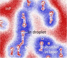
Abstract Vacuum sublimated III–V semiconductor surfaces are often rough and populated by III droplets with little known about the areas in between. Using in situ spectromicroscopy, the sublimation and recrystallization of InP(100) surfaces are followed and controlled in real time, revealing unexpectedly the presence of an ultrathin In layer that coexists with microscopic In droplets. The In layer can be enticed to dewet by controlled exposure to ultraviolet photons which induce quantum electronic stress in the layer. Dewetted atoms redistribute toward existing droplets, forming ultrathin layers around them. Upon heating the layers expand and overlap to form a contiguous layer, returning the surface to the original state prior to dewetting. Effectively, ultrathin In layer can be grown and broken up at will. The wetting-dewetting dynamics around intrinsic (In) and extrinsic (Au) droplets are observed in situ via low-energy electron microscopy while chemical analyses of the surfaces are made using synchrotron-based soft X-rays photoemission electron microscopy. The results demonstrate the often overlooked possibility to grow flat, ultrathin metal films on semiconductors, despite lattice mismatch and the close-packed nature of metallic bond. Ultrathin In layers also offer a unique system to advance experimental studies of two-dimensional superconductivity.
中文翻译:

升华InP(100)表面超薄In层的原位观察和控制
摘要真空升华的 III-V 族半导体表面通常是粗糙的,并且由 III 级液滴填充,而对其之间的区域知之甚少。使用原位光谱显微镜,实时跟踪和控制 InP(100) 表面的升华和重结晶,意外地揭示了与微观 In 液滴共存的超薄 In 层的存在。In 层可以通过受控暴露于紫外线光子来引诱去湿,紫外线光子会在该层中引起量子电子应力。去湿的原子重新分布到现有的液滴中,在它们周围形成超薄层。加热后,这些层会膨胀并重叠形成一个连续的层,使表面恢复到去湿前的原始状态。有效地,超薄In层可以随意生长和分解。通过低能电子显微镜原位观察内在 (In) 和外在 (Au) 液滴周围的润湿-去润湿动力学,而使用基于同步加速器的软 X 射线光电电子显微镜对表面进行化学分析。结果表明,尽管晶格失配和金属键的密堆积性质,在半导体上生长平坦的超薄金属薄膜的可能性经常被忽视。超薄 In 层还提供了一个独特的系统来推进二维超导性的实验研究。尽管晶格失配和金属键的密堆积性质,半导体上的超薄金属薄膜。超薄 In 层还提供了一个独特的系统来推进二维超导性的实验研究。尽管晶格失配和金属键的密堆积性质,半导体上的超薄金属薄膜。超薄 In 层还提供了一个独特的系统来推进二维超导性的实验研究。
更新日期:2021-03-01
中文翻译:
升华InP(100)表面超薄In层的原位观察和控制
摘要真空升华的 III-V 族半导体表面通常是粗糙的,并且由 III 级液滴填充,而对其之间的区域知之甚少。使用原位光谱显微镜,实时跟踪和控制 InP(100) 表面的升华和重结晶,意外地揭示了与微观 In 液滴共存的超薄 In 层的存在。In 层可以通过受控暴露于紫外线光子来引诱去湿,紫外线光子会在该层中引起量子电子应力。去湿的原子重新分布到现有的液滴中,在它们周围形成超薄层。加热后,这些层会膨胀并重叠形成一个连续的层,使表面恢复到去湿前的原始状态。有效地,超薄In层可以随意生长和分解。通过低能电子显微镜原位观察内在 (In) 和外在 (Au) 液滴周围的润湿-去润湿动力学,而使用基于同步加速器的软 X 射线光电电子显微镜对表面进行化学分析。结果表明,尽管晶格失配和金属键的密堆积性质,在半导体上生长平坦的超薄金属薄膜的可能性经常被忽视。超薄 In 层还提供了一个独特的系统来推进二维超导性的实验研究。尽管晶格失配和金属键的密堆积性质,半导体上的超薄金属薄膜。超薄 In 层还提供了一个独特的系统来推进二维超导性的实验研究。尽管晶格失配和金属键的密堆积性质,半导体上的超薄金属薄膜。超薄 In 层还提供了一个独特的系统来推进二维超导性的实验研究。


 京公网安备 11010802027423号