当前位置:
X-MOL 学术
›
ACS Appl. Nano Mater.
›
论文详情
Our official English website, www.x-mol.net, welcomes your
feedback! (Note: you will need to create a separate account there.)
Multilayer GaSe/InSe Heterointerface-Based Devices for Charge Transport and Optoelectronics
ACS Applied Nano Materials ( IF 5.3 ) Pub Date : 2020-11-25 , DOI: 10.1021/acsanm.0c02280 Yi-Ying Lu, Chuan-Ruei Guo, Hui-Lin Yeh, He-Wen Chen, Chien-Cheng Kuo, Jui-Hung Hsu, Jie Jhou, Yan-Ting Huang, Shang-Hsien Hsieh, Chia-Hao Chen, Ching-Hwa Ho, Raman Sankar, Fang-Cheng Chou
ACS Applied Nano Materials ( IF 5.3 ) Pub Date : 2020-11-25 , DOI: 10.1021/acsanm.0c02280 Yi-Ying Lu, Chuan-Ruei Guo, Hui-Lin Yeh, He-Wen Chen, Chien-Cheng Kuo, Jui-Hung Hsu, Jie Jhou, Yan-Ting Huang, Shang-Hsien Hsieh, Chia-Hao Chen, Ching-Hwa Ho, Raman Sankar, Fang-Cheng Chou
|
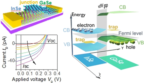
Interface interactions between two distinct layered materials of vertically stacked van der Waals (vdW) heterostructures play a vital role in the modulation of their electrical/optoelectronic properties. Meanwhile, intriguing properties, e.g., ultrafast charge transfer (Jin Nat Nanotechnol., 2018, 13, 994−1003) and moiré excitons (Tran et al Nature, 2019, 567, 71−75), have been discovered in strongly coupled heterobilayers composed of transition metal dichalcogenides; post-transition metal chalcogenides GaSe and InSe remain unexplored. Here, we use photoluminescence measurements and a scanning photoelectron microscope for electronic characterization of multilayer vertically stacked GaSe/InSe samples coupled with two-probe electrical measurements to reveal the carrier transport and optoelectronic properties at a strongly coupled GaSe/InSe vdW interface. A significant PL quenching and a shift of the valence band with respect to the Fermi level occurred at the heterojunction, evidencing the strong coupling of charge transfer between the GaSe and InSe layers. The band alignment at this heterointerface was determined as a type-II band alignment, similar to a weakly coupled system; however, charge transfer led to charge redistribution in the vicinity of the heterointerface, resulting in an interface dipole. Strong interface coupling also made the origin of the forward current different from that of the weakly coupled system; it is governed by interlayer recombination between the majority carriers rather than carrier injection over conduction band offsets. Moreover, tuning the band alignment via modulation of the majority carriers could further change the origin of the photocurrent. Our results not only present the first charge transport study of a strongly coupled multilayer GaSe/InSe system but also open up the way to further utilizing vdW interfaces in the applications of next-generation optoelectronics.
中文翻译:

基于多层GaSe / InSe异质界面的器件,用于电荷传输和光电
垂直堆叠的范德华(vdW)异质结构的两种不同层状材料之间的界面相互作用在其电/光电子特性的调制中起着至关重要的作用。同时,令人着迷的特性,例如超快速电荷转移(斤 Nat纳米技术。, 2018, 13,994-1003)和波纹线态激子(特兰 等自然,2019,567(71-75),已经发现在由过渡金属二卤化物组成的强耦合异质双层中;过渡后金属硫族化物GaSe和InSe尚未开发。在这里,我们使用光致发光测量和扫描光电子显微镜对多层垂直堆叠的GaSe / InSe样品进行电子表征,并结合双探针电测量,以揭示在强耦合的GaSe / InSe vdW接口处的载流子传输和光电性能。在异质结处发生了显着的PL猝灭和价带相对于费米能级的移动,证明了GaSe和InSe层之间电荷转移的强耦合。类似于弱耦合系统,该异质界面处的能带对准被确定为II型能带对准。然而,电荷转移导致异质界面附近的电荷重新分布,从而导致界面偶极子。强的接口耦合也使正向电流的起源不同于弱耦合的系统。它是由多数载流子之间的层间复合而不是载流子在导带偏移上注入所决定的。而且,通过多数载流子的调制来调整带对准可以进一步改变光电流的起源。我们的研究结果不仅是对强耦合多层GaSe / InSe系统进行的首次电荷传输研究,而且还为在下一代光电应用中进一步利用vdW接口开辟了道路。强的接口耦合也使正向电流的起源不同于弱耦合的系统。它是由多数载流子之间的层间复合而不是载流子在导带偏移上注入所决定的。而且,通过多数载流子的调制来调整带对准可以进一步改变光电流的起源。我们的研究结果不仅是对强耦合多层GaSe / InSe系统进行的首次电荷传输研究,而且还为在下一代光电应用中进一步利用vdW接口开辟了道路。强的接口耦合也使正向电流的起源不同于弱耦合的系统。它是由多数载流子之间的层间复合而不是载流子在导带偏移上注入所决定的。而且,通过多数载流子的调制来调整带对准可以进一步改变光电流的起源。我们的研究结果不仅是对强耦合多层GaSe / InSe系统进行的首次电荷传输研究,而且还为在下一代光电应用中进一步利用vdW接口开辟了道路。通过多数载流子的调制来调整频带对准可以进一步改变光电流的起源。我们的研究结果不仅是对强耦合多层GaSe / InSe系统进行的首次电荷传输研究,而且还为在下一代光电应用中进一步利用vdW接口开辟了道路。通过多数载流子的调制来调整频带对准可以进一步改变光电流的起源。我们的研究结果不仅是对强耦合多层GaSe / InSe系统进行的首次电荷传输研究,而且还为在下一代光电应用中进一步利用vdW接口开辟了道路。
更新日期:2020-12-24
中文翻译:
基于多层GaSe / InSe异质界面的器件,用于电荷传输和光电
垂直堆叠的范德华(vdW)异质结构的两种不同层状材料之间的界面相互作用在其电/光电子特性的调制中起着至关重要的作用。同时,令人着迷的特性,例如超快速电荷转移(


 京公网安备 11010802027423号