当前位置:
X-MOL 学术
›
Mater. Chem. Phys.
›
论文详情
Our official English website, www.x-mol.net, welcomes your
feedback! (Note: you will need to create a separate account there.)
Electrochemical imprint lithography on Si surface using a patterned polymer electrolyte membrane
Materials Chemistry and Physics ( IF 4.3 ) Pub Date : 2021-02-01 , DOI: 10.1016/j.matchemphys.2020.124081 Ryohei Umezaki , Junji Murata
Materials Chemistry and Physics ( IF 4.3 ) Pub Date : 2021-02-01 , DOI: 10.1016/j.matchemphys.2020.124081 Ryohei Umezaki , Junji Murata
|
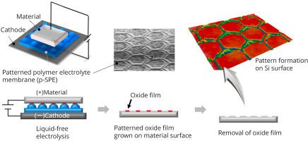
Abstract Well-defined surface patterns can be applied to improve surface characteristics, optical properties, and wettability. Electrochemical imprint lithography is a promising method for fabricating micro/nanostructural patterns on material surfaces through low-cost procedures. However, this method typically requires a large amount of electrolyte and a complex electrochemical setup. Herein, we present a novel liquid-electrolyte-free electrochemical imprint lithography method involving the use of a patterned Nafion polymer electrolyte membrane. In this method, the Si material surface in contact with the patterned Nafion membrane is selectively oxidized through a liquid-electrolyte-free electrochemical method. Following the removal of the resulting oxide film by HF dipping, patterned structures with a width of 70–170 μm and a depth of 40 nm can be obtained on the Si surface. The etching depth increases proportionally with the electrolysis time. The presence of a liquid electrolyte between the Si surface and the Nafion membrane during electrolysis increases the width of the pattern formed on the Si surface. This indicates that the liquid-electrolyte-free electrochemical method facilitates more accurate pattern transformation on the Si surface than that involving the use of a liquid electrolyte. The dotted, hexagonal, and lattice patterned Si surfaces can be fabricated at room temperature by using the proposed method. The proposed liquid-electrolyte-free electrochemical imprint lithography method involving the use of a patterned Nafion membrane is a simple, environment-friendly direct imprinting process that can be applied for micropatterning on and surface functionalization of hard and stable materials.
中文翻译:

使用图案化聚合物电解质膜在硅表面上进行电化学压印光刻
摘要 定义明确的表面图案可用于改善表面特性、光学特性和润湿性。电化学压印光刻是一种通过低成本程序在材料表面制造微/纳米结构图案的有前途的方法。然而,这种方法通常需要大量的电解质和复杂的电化学装置。在此,我们提出了一种新型的无液体电解质电化学压印光刻方法,该方法涉及使用图案化的 Nafion 聚合物电解质膜。在该方法中,与图案化的 Nafion 膜接触的 Si 材料表面通过无液体电解质的电化学方法被选择性氧化。通过 HF 浸渍去除生成的氧化膜后,可以在 Si 表面获得宽度为 70-170 μm 和深度为 40 nm 的图案结构。蚀刻深度与电解时间成正比。在电解过程中,Si 表面和 Nafion 膜之间存在液体电解质会增加在 Si 表面上形成的图案的宽度。这表明,与使用液体电解质的方法相比,无液体电解质的电化学方法有助于在 Si 表面上进行更准确的图案转换。通过使用所提出的方法,可以在室温下制造点状、六边形和晶格图案化的 Si 表面。所提出的涉及使用图案化 Nafion 膜的无液体电解质电化学压印光刻方法是一种简单、
更新日期:2021-02-01
中文翻译:
使用图案化聚合物电解质膜在硅表面上进行电化学压印光刻
摘要 定义明确的表面图案可用于改善表面特性、光学特性和润湿性。电化学压印光刻是一种通过低成本程序在材料表面制造微/纳米结构图案的有前途的方法。然而,这种方法通常需要大量的电解质和复杂的电化学装置。在此,我们提出了一种新型的无液体电解质电化学压印光刻方法,该方法涉及使用图案化的 Nafion 聚合物电解质膜。在该方法中,与图案化的 Nafion 膜接触的 Si 材料表面通过无液体电解质的电化学方法被选择性氧化。通过 HF 浸渍去除生成的氧化膜后,可以在 Si 表面获得宽度为 70-170 μm 和深度为 40 nm 的图案结构。蚀刻深度与电解时间成正比。在电解过程中,Si 表面和 Nafion 膜之间存在液体电解质会增加在 Si 表面上形成的图案的宽度。这表明,与使用液体电解质的方法相比,无液体电解质的电化学方法有助于在 Si 表面上进行更准确的图案转换。通过使用所提出的方法,可以在室温下制造点状、六边形和晶格图案化的 Si 表面。所提出的涉及使用图案化 Nafion 膜的无液体电解质电化学压印光刻方法是一种简单、


 京公网安备 11010802027423号