当前位置:
X-MOL 学术
›
Adv. Mater. Interfaces
›
论文详情
Our official English website, www.x-mol.net, welcomes your
feedback! (Note: you will need to create a separate account there.)
Selective Area Growth and Transfer of High Optical Quality MoS2 Layers
Advanced Materials Interfaces ( IF 4.3 ) Pub Date : 2020-11-23 , DOI: 10.1002/admi.202001549 Pranab K. Mohapatra 1 , Kamalakannan Ranganathan 1 , Ariel Ismach 1
Advanced Materials Interfaces ( IF 4.3 ) Pub Date : 2020-11-23 , DOI: 10.1002/admi.202001549 Pranab K. Mohapatra 1 , Kamalakannan Ranganathan 1 , Ariel Ismach 1
Affiliation
|
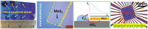
This study demonstrates that monolayer molybdenum disulfide (MoS2) can be grown on selective areas of a substrate by creating isolated microcavity reactors throughout the substrate in a chemical vapor deposition (CVD) process. The obtained MoS2 in the confined areas can be tuned from isolated triangular domains of few tens of microns to a continuous film with different thicknesses by modulating the growth parameters. In contrast, the growth on the open areas of the substrate leads to an inhomogeneous film. Using the confined‐CVD approach, the area‐selective growth of MoS2 domains and films on arbitrary substrates such as SiO2/Si, sapphire, gold‐patterned SiO2/Si substrates, and SiNx‐membrane‐supported TEM grid is shown. Raman and photoluminescence spectroscopy studies reveal that the confined‐CVD‐derived MoS2 layers have high crystal quality and superior optical performance when compared to mechanically exfoliated flakes. A novel and efficient methodology is further introduced for the selective transfer of the confined‐growth areas to pre‐patterned substrates, therefore allowing multiple use of a single growth sample. Finally, field‐effect transistor devices are made on individual domains and mobilities up to ≈6.8 cm2 V−1 s−1 measured. The confined‐CVD approach and the selective area transfer presented here can be implemented on other transition metal dichalcogenides and 2D materials in general.
中文翻译:

选择性区域的生长和高质量光学MoS2层的转移
这项研究表明,通过在化学气相沉积(CVD)过程中在整个基板上创建隔离的微腔反应器,可以在基板的选择性区域上生长单层二硫化钼(MoS 2)。可以通过调节生长参数将密闭区域中获得的MoS 2从几十微米的孤立三角区域调整为具有不同厚度的连续膜。相反,在基板的开口区域上的生长导致不均匀的膜。使用受限CVD方法,可以在任意衬底(例如SiO 2 / Si,蓝宝石,金图案化的SiO 2 / Si衬底和SiN x)上对MoS 2域和膜进行区域选择性生长显示了膜支持的TEM网格。拉曼光谱和光致发光光谱研究表明,与机械剥离的薄片相比,有限的CVD衍生的MoS 2层具有较高的晶体质量和优异的光学性能。进一步引入了一种新颖而有效的方法,用于将密闭生长区域选择性转移到预先形成图案的底物上,因此允许多次使用单个生长样品。最后,在各个域上制作了场效应晶体管器件,迁移率高达≈6.8cm 2 V -1 s -1。此处介绍的受限CVD方法和选择性区域转移通常可以在其他过渡金属二卤化物和2D材料上实现。
更新日期:2020-12-17
中文翻译:
选择性区域的生长和高质量光学MoS2层的转移
这项研究表明,通过在化学气相沉积(CVD)过程中在整个基板上创建隔离的微腔反应器,可以在基板的选择性区域上生长单层二硫化钼(MoS 2)。可以通过调节生长参数将密闭区域中获得的MoS 2从几十微米的孤立三角区域调整为具有不同厚度的连续膜。相反,在基板的开口区域上的生长导致不均匀的膜。使用受限CVD方法,可以在任意衬底(例如SiO 2 / Si,蓝宝石,金图案化的SiO 2 / Si衬底和SiN x)上对MoS 2域和膜进行区域选择性生长显示了膜支持的TEM网格。拉曼光谱和光致发光光谱研究表明,与机械剥离的薄片相比,有限的CVD衍生的MoS 2层具有较高的晶体质量和优异的光学性能。进一步引入了一种新颖而有效的方法,用于将密闭生长区域选择性转移到预先形成图案的底物上,因此允许多次使用单个生长样品。最后,在各个域上制作了场效应晶体管器件,迁移率高达≈6.8cm 2 V -1 s -1。此处介绍的受限CVD方法和选择性区域转移通常可以在其他过渡金属二卤化物和2D材料上实现。


 京公网安备 11010802027423号