当前位置:
X-MOL 学术
›
Mater. Chem. Phys.
›
论文详情
Our official English website, www.x-mol.net, welcomes your
feedback! (Note: you will need to create a separate account there.)
Influence of Thickness on Crystallographic, Stereometric, Optoelectronic, and Electrochemical Characteristics of Electron-Beam Deposited Indium Tin Oxide thin Films
Materials Chemistry and Physics ( IF 4.3 ) Pub Date : 2021-02-01 , DOI: 10.1016/j.matchemphys.2020.124051 Fatemeh Ghamari , Davood Raoufi , Jalal Arjomandi
Materials Chemistry and Physics ( IF 4.3 ) Pub Date : 2021-02-01 , DOI: 10.1016/j.matchemphys.2020.124051 Fatemeh Ghamari , Davood Raoufi , Jalal Arjomandi
|
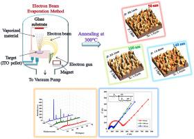
Abstract High transparency, low resistivity, and smooth surface of transparent conductive oxides like ITO (Indium Tin Oxide) thin films yet are desired for achieving diverse fields of optoelectronic and energy storage usages. Here, it was illustrated how the thickness variations of ITO films during deposition onto a substrate of glass through the electron beam evaporation method could influence the main features of the films. For acquiring this goal, besides optoelectronic, crystallographic and stereometric analyses of surface morphology, electrochemical investigations of the films were performed. X-ray diffraction or XRD results of ITO films revealed along with growth processing, crystallite size value, inter-planar spacing, and lattice constant increased. However, strain, dislocation density, and texture coefficient of the films showed a different trend. The maximum crystalline size (41 nm) and minimum micro-strain (3.1939 × 10⁻³) were observed in the thickest ITO film (140 nm). Spectroscopic data confirmed the lowering transparency of ITO films during the growth of thicknesses (from 95.56 %to 82.50 %). The conductivity examinations of the films revealed with increasing the thickness, sheet resistance decreased. The highest resistivity was related to 50 nm ITO film, 79 Ω/□, while the resistance of the ITO film with 140 nm thickness was 32 Ω/□. Functional surface and volume parameters results as well as monofractal dimension outcomes, derived from atomic force microscopy (AFM) data, described the thicker ITO films had smoother surface and lower porosity. Furthermore, the electrochemical analyses include electrochemical impedance spectroscopy and cyclic voltammetry studies verified the increasing the conductivity of the films during thickness growth.
中文翻译:

厚度对电子束沉积氧化铟锡薄膜的晶体学、立体测量、光电和电化学特性的影响
摘要 透明导电氧化物如 ITO(氧化铟锡)薄膜的高透明度、低电阻率和光滑的表面是实现光电和储能应用的不同领域所需要的。在这里,说明了在通过电子束蒸发方法沉积到玻璃基板上期间 ITO 薄膜的厚度变化如何影响薄膜的主要特征。为了实现这一目标,除了对表面形态进行光电、晶体学和立体测量分析外,还对薄膜进行了电化学研究。ITO 薄膜的 X 射线衍射或 XRD 结果显示随着生长过程、微晶尺寸值、面间距和晶格常数的增加。然而,应变、位错密度、薄膜的织构系数呈现不同的趋势。在最厚的 ITO 薄膜 (140 nm) 中观察到最大晶体尺寸 (41 nm) 和最小微应变 (3.1939 × 10⁻³)。光谱数据证实了 ITO 薄膜在厚度增长过程中的透明度降低(从 95.56 % 到 82.50 %)。薄膜的电导率检测表明,随着厚度的增加,薄层电阻降低。最高电阻率与50 nm ITO膜有关,79 Ω/□,而140 nm厚度的ITO膜的电阻为32 Ω/□。来自原子力显微镜 (AFM) 数据的功能表面和体积参数结果以及单分形维数结果表明,较厚的 ITO 薄膜具有更光滑的表面和更低的孔隙率。此外,
更新日期:2021-02-01
中文翻译:
厚度对电子束沉积氧化铟锡薄膜的晶体学、立体测量、光电和电化学特性的影响
摘要 透明导电氧化物如 ITO(氧化铟锡)薄膜的高透明度、低电阻率和光滑的表面是实现光电和储能应用的不同领域所需要的。在这里,说明了在通过电子束蒸发方法沉积到玻璃基板上期间 ITO 薄膜的厚度变化如何影响薄膜的主要特征。为了实现这一目标,除了对表面形态进行光电、晶体学和立体测量分析外,还对薄膜进行了电化学研究。ITO 薄膜的 X 射线衍射或 XRD 结果显示随着生长过程、微晶尺寸值、面间距和晶格常数的增加。然而,应变、位错密度、薄膜的织构系数呈现不同的趋势。在最厚的 ITO 薄膜 (140 nm) 中观察到最大晶体尺寸 (41 nm) 和最小微应变 (3.1939 × 10⁻³)。光谱数据证实了 ITO 薄膜在厚度增长过程中的透明度降低(从 95.56 % 到 82.50 %)。薄膜的电导率检测表明,随着厚度的增加,薄层电阻降低。最高电阻率与50 nm ITO膜有关,79 Ω/□,而140 nm厚度的ITO膜的电阻为32 Ω/□。来自原子力显微镜 (AFM) 数据的功能表面和体积参数结果以及单分形维数结果表明,较厚的 ITO 薄膜具有更光滑的表面和更低的孔隙率。此外,


 京公网安备 11010802027423号