当前位置:
X-MOL 学术
›
Adv. Mater.
›
论文详情
Our official English website, www.x-mol.net, welcomes your
feedback! (Note: you will need to create a separate account there.)
Tailored Graphene Micropatterns by Wafer‐Scale Direct Transfer for Flexible Chemical Sensor Platform
Advanced Materials ( IF 27.4 ) Pub Date : 2020-11-20 , DOI: 10.1002/adma.202004827 Yeonhoo Kim 1, 2 , Taehoon Kim 1 , Jinwoo Lee 3 , Yong Seok Choi 4 , Joonhee Moon 5 , Seo Yun Park 1 , Tae Hyung Lee 1 , Hoon Kee Park 1 , Sol A Lee 1 , Min Sang Kwon 1 , Hyung‐Gi Byun 6 , Jong‐Heun Lee 7 , Myoung‐Gyu Lee 1 , Byung Hee Hong 4, 8 , Ho Won Jang 1
Advanced Materials ( IF 27.4 ) Pub Date : 2020-11-20 , DOI: 10.1002/adma.202004827 Yeonhoo Kim 1, 2 , Taehoon Kim 1 , Jinwoo Lee 3 , Yong Seok Choi 4 , Joonhee Moon 5 , Seo Yun Park 1 , Tae Hyung Lee 1 , Hoon Kee Park 1 , Sol A Lee 1 , Min Sang Kwon 1 , Hyung‐Gi Byun 6 , Jong‐Heun Lee 7 , Myoung‐Gyu Lee 1 , Byung Hee Hong 4, 8 , Ho Won Jang 1
Affiliation
|
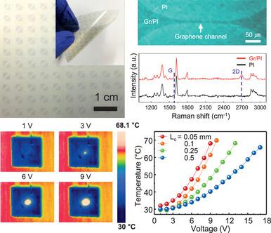
2D materials, such as graphene, exhibit great potential as functional materials for numerous novel applications due to their excellent properties. The grafting of conventional micropatterning techniques on new types of electronic devices is required to fully utilize the unique nature of graphene. However, the conventional lithography and polymer‐supported transfer methods often induce the contamination and damage of the graphene surface due to polymer residues and harsh wet‐transfer conditions. Herein, a novel strategy to obtain micropatterned graphene on polymer substrates using a direct curing process is demonstrated. Employing this method, entirely flexible, transparent, well‐defined self‐activated graphene sensor arrays, capable of gas discrimination without external heating, are fabricated on 4 in. wafer‐scale substrates. Finite element method simulations show the potential of this patterning technique to maximize the performance of the sensor devices when the active channels of the 2D material are suspended and nanoscaled. This study contributes considerably to the development of flexible functional electronic devices based on 2D materials.
中文翻译:

晶圆级直接转移量身定制的石墨烯微图案,用于柔性化学传感器平台
诸如石墨烯之类的2D材料由于其优异的性能而具有作为许多新型应用的功能材料的巨大潜力。为了充分利用石墨烯的独特性质,需要将传统的微图案技术嫁接到新型的电子设备上。但是,由于聚合物残留物和苛刻的湿转移条件,传统的光刻和聚合物支撑的转移方法经常会引起石墨烯表面的污染和损坏。在本文中,展示了一种使用直接固化工艺在聚合物基材上获得微图案化石墨烯的新颖策略。采用这种方法,可以在4英寸晶圆级基板上制造出完全灵活,透明,定义明确的自激活石墨烯传感器阵列,无需外部加热即可识别气体。有限元方法仿真表明,当2D材料的有源通道被悬挂并纳米级化时,这种图案化技术有潜力使传感器设备的性能最大化。这项研究为基于2D材料的柔性功能电子设备的开发做出了巨大贡献。
更新日期:2021-01-12
中文翻译:
晶圆级直接转移量身定制的石墨烯微图案,用于柔性化学传感器平台
诸如石墨烯之类的2D材料由于其优异的性能而具有作为许多新型应用的功能材料的巨大潜力。为了充分利用石墨烯的独特性质,需要将传统的微图案技术嫁接到新型的电子设备上。但是,由于聚合物残留物和苛刻的湿转移条件,传统的光刻和聚合物支撑的转移方法经常会引起石墨烯表面的污染和损坏。在本文中,展示了一种使用直接固化工艺在聚合物基材上获得微图案化石墨烯的新颖策略。采用这种方法,可以在4英寸晶圆级基板上制造出完全灵活,透明,定义明确的自激活石墨烯传感器阵列,无需外部加热即可识别气体。有限元方法仿真表明,当2D材料的有源通道被悬挂并纳米级化时,这种图案化技术有潜力使传感器设备的性能最大化。这项研究为基于2D材料的柔性功能电子设备的开发做出了巨大贡献。


 京公网安备 11010802027423号