当前位置:
X-MOL 学术
›
Appl. Surf. Sci.
›
论文详情
Our official English website, www.x-mol.net, welcomes your
feedback! (Note: you will need to create a separate account there.)
TiO2-SiO2 mixed oxide deposited by low pressure PECVD: insights on optical and nanoscale electrical properties
Applied Surface Science ( IF 6.3 ) Pub Date : 2021-03-01 , DOI: 10.1016/j.apsusc.2020.148510 M. Mitronika , C. Villeneuve-Faure , F. Massol , L. Boudou , W. Ravisy , M.P. Besland , A. Goullet , M. Richard-Plouet
Applied Surface Science ( IF 6.3 ) Pub Date : 2021-03-01 , DOI: 10.1016/j.apsusc.2020.148510 M. Mitronika , C. Villeneuve-Faure , F. Massol , L. Boudou , W. Ravisy , M.P. Besland , A. Goullet , M. Richard-Plouet
|
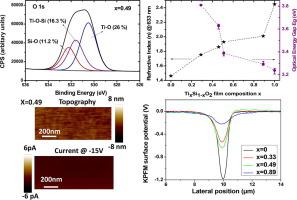
Abstract TixSi1-xO2 thin films appear as promising materials to replace SiO2 for DRAM devices. For the effective down scaling, these mixed oxides should combine the best properties from SiO2 (low leakage current) and TiO2 (high dielectric constant). In this study, TixSi1-xO2 thin films were deposited by low pressure PECVD. Varying the Titanium Tetra-Isopropoxide (TTIP) and Hexamethyldisiloxane (HMDSO) precursors flow rate allows us to obtain nanostructured films with tunable properties. Their surface chemical composition was assessed by X-ray Photoelectron Spectroscopy (XPS). Atomic Force Microscopy (AFM) revealed that the surface roughness increases with the Ti content. Spectroscopic Ellipsometry (SE) showed that a small amount of Ti is enough to induce a decrease of the energy gap and an increase of the refractive index, while preserving a low surface roughness. Since these mixed oxide films exhibit nanodomains with three different environments with randomly distributed Si-O-Ti bonds, SiO2-like and TiO2-like bonds, electrical properties are investigated at nanoscale in terms of dielectric permittivity, charge injection, trapping and transport via electrical modes derived from AFM as Electrostatic Force Microscopy (EFM), Kelvin Force Probe Microscopy (KPFM) and Conductive AFM (C-AFM). Despite a chemical composition evolving at the nanoscale, this work highlights that the electrical behavior can be considered as homogeneous (at the AFM resolution scale). A small amount of Ti induces a decrease in the amount of trapped electrons due to charge transport increase and a strong decrease of trapped holes. Moreover, after injection, the rate of charge decay increases with the Ti content. These features were interpreted on the basis of the energy diagrams deduced from the Valence Band measurement highlighting the n-type semiconducting character of the Ti-rich films. As a conclusion, TixSi1-xO2 films with x=0.33 allows the best compromise in terms of dielectric permittivity improvement, charge injection and transport behavior.
中文翻译:

通过低压 PECVD 沉积的 TiO2-SiO2 混合氧化物:对光学和纳米级电学特性的见解
摘要 TixSi1-xO2 薄膜有望成为 DRAM 器件中替代 SiO2 的材料。为了有效缩小尺寸,这些混合氧化物应结合 SiO2(低漏电流)和 TiO2(高介电常数)的最佳特性。在这项研究中,TixSi1-xO2 薄膜是通过低压 PECVD 沉积的。改变四异丙氧基钛 (TTIP) 和六甲基二硅氧烷 (HMDSO) 前体的流速使我们能够获得具有可调特性的纳米结构薄膜。它们的表面化学成分通过 X 射线光电子能谱 (XPS) 进行评估。原子力显微镜 (AFM) 显示表面粗糙度随着 Ti 含量的增加而增加。光谱椭偏仪 (SE) 表明少量的 Ti 足以引起能隙的减小和折射率的增加,同时保持较低的表面粗糙度。由于这些混合氧化物薄膜呈现出具有随机分布的 Si-O-Ti 键、SiO2 类和 TiO2 类键的三种不同环境的纳米域,因此在纳米尺度上研究了介电常数、电荷注入、捕获和通过电传输的电学特性。源自 AFM 的模式,如静电力显微镜 (EFM)、开尔文力探针显微镜 (KPFM) 和导电 AFM (C-AFM)。尽管化学成分在纳米尺度上演变,但这项工作强调了电行为可以被认为是均匀的(在 AFM 分辨率尺度上)。由于电荷传输的增加和被困空穴的强烈减少,少量的 Ti 会导致被俘获电子的数量减少。此外,注射后,电荷衰减率随着 Ti 含量的增加而增加。这些特征是根据价带测量推导出的能量图来解释的,这些图突出了富钛薄膜的 n 型半导体特性。总之,x=0.33 的 TixSi1-xO2 薄膜在介电常数改善、电荷注入和传输行为方面实现了最佳折衷。
更新日期:2021-03-01
中文翻译:
通过低压 PECVD 沉积的 TiO2-SiO2 混合氧化物:对光学和纳米级电学特性的见解
摘要 TixSi1-xO2 薄膜有望成为 DRAM 器件中替代 SiO2 的材料。为了有效缩小尺寸,这些混合氧化物应结合 SiO2(低漏电流)和 TiO2(高介电常数)的最佳特性。在这项研究中,TixSi1-xO2 薄膜是通过低压 PECVD 沉积的。改变四异丙氧基钛 (TTIP) 和六甲基二硅氧烷 (HMDSO) 前体的流速使我们能够获得具有可调特性的纳米结构薄膜。它们的表面化学成分通过 X 射线光电子能谱 (XPS) 进行评估。原子力显微镜 (AFM) 显示表面粗糙度随着 Ti 含量的增加而增加。光谱椭偏仪 (SE) 表明少量的 Ti 足以引起能隙的减小和折射率的增加,同时保持较低的表面粗糙度。由于这些混合氧化物薄膜呈现出具有随机分布的 Si-O-Ti 键、SiO2 类和 TiO2 类键的三种不同环境的纳米域,因此在纳米尺度上研究了介电常数、电荷注入、捕获和通过电传输的电学特性。源自 AFM 的模式,如静电力显微镜 (EFM)、开尔文力探针显微镜 (KPFM) 和导电 AFM (C-AFM)。尽管化学成分在纳米尺度上演变,但这项工作强调了电行为可以被认为是均匀的(在 AFM 分辨率尺度上)。由于电荷传输的增加和被困空穴的强烈减少,少量的 Ti 会导致被俘获电子的数量减少。此外,注射后,电荷衰减率随着 Ti 含量的增加而增加。这些特征是根据价带测量推导出的能量图来解释的,这些图突出了富钛薄膜的 n 型半导体特性。总之,x=0.33 的 TixSi1-xO2 薄膜在介电常数改善、电荷注入和传输行为方面实现了最佳折衷。


 京公网安备 11010802027423号