当前位置:
X-MOL 学术
›
Prog. Photovoltaics
›
论文详情
Our official English website, www.x-mol.net, welcomes your
feedback! (Note: you will need to create a separate account there.)
Rear interface engineering of kesterite Cu2ZnSnSe4 solar cells by adding CuGaSe2 thin layers
Progress in Photovoltaics ( IF 8.0 ) Pub Date : 2020-11-18 , DOI: 10.1002/pip.3366 Sergio Giraldo 1 , Robert Fonoll‐Rubio 1 , Zacharie Jehl Li‐Kao 1 , Yudania Sánchez 1 , Lorenzo Calvo‐Barrio 2, 3 , Victor Izquierdo‐Roca 1 , Alejandro Pérez‐Rodríguez 1, 3 , Edgardo Saucedo 1
Progress in Photovoltaics ( IF 8.0 ) Pub Date : 2020-11-18 , DOI: 10.1002/pip.3366 Sergio Giraldo 1 , Robert Fonoll‐Rubio 1 , Zacharie Jehl Li‐Kao 1 , Yudania Sánchez 1 , Lorenzo Calvo‐Barrio 2, 3 , Victor Izquierdo‐Roca 1 , Alejandro Pérez‐Rodríguez 1, 3 , Edgardo Saucedo 1
Affiliation
|
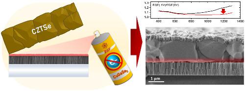
Kesterite Cu2ZnSn(S,Se)4 thin film technology has been thoroughly investigated during the last decade as a promising solution in the field of low‐cost, sustainable, and environmental‐friendly photovoltaic technologies. However, despite efforts to boost kesterite solar cells performance by numerous strategies, the efficiencies remain stagnant around 13%. Some commonly observed issues in this technology refer to recombination events due to the likely presence of defects and, largely in line with the latest, the presence of voids and poor morphologies at the rear interface. This work, partly inspired by the copper indium gallium selenide (CIGS) technology and the use of wide‐bandgap Ga‐rich region as back surface field (BSF), focuses on an innovative approach using ultrathin CuGa layers at the rear interface to promote the formation of wide‐bandgap CuGaSe2, acting as an efficient electron reflector or BSF, and to function as an effective interlayer improving the kesterite crystallinity at the back interface. Kesterite Cu2ZnSnSe4 devices fabricated with added CuGa layers show a general increase in photovoltaic parameters and a significantly enhanced collection efficiency compared with reference devices without CuGa. This strategy proves to be successful, for not only passivating but also for improving the Mo/kesterite interface morphology, preventing to a large extent the presence of voids at the back region of the absorber.
中文翻译:

通过添加CuGaSe2薄层对Kesterite Cu2ZnSnSe4太阳能电池进行后接口工程
Kesterite Cu 2 ZnSn(S,Se)4在过去的十年中,对薄膜技术进行了彻底的研究,作为低成本,可持续发展和环境友好型光伏技术领域中的一种有前途的解决方案。然而,尽管通过多种策略努力提高了硅藻土太阳能电池的性能,但效率仍然停滞在13%左右。由于可能存在缺陷,并且由于与最新技术相一致,后接口处存在空隙和不良的形态,因此该技术中一些通常观察到的问题指的是重组事件。这项工作部分地受到硒化铜铟镓(CIGS)技术的启发,并利用宽带隙丰富的Ga富集区域作为背面场(BSF),其工作重点是在后界面使用超薄CuGa层来促进半导体材料的创新方法。带隙CuGaSe的形成如图2所示,其用作有效的电子反射器或BSF,并用作改善后界面处的硅藻土结晶度的有效中间层。与没有CuGa的参考器件相比,添加了CuGa层的Kesterite Cu 2 ZnSnSe 4器件显示出光伏参数的普遍增加,并且收集效率显着提高。事实证明,该策略是成功的,不仅钝化而且还改善了Mo / kesterite界面形态,并在很大程度上防止了吸收体背面的空隙。
更新日期:2020-11-18
中文翻译:
通过添加CuGaSe2薄层对Kesterite Cu2ZnSnSe4太阳能电池进行后接口工程
Kesterite Cu 2 ZnSn(S,Se)4在过去的十年中,对薄膜技术进行了彻底的研究,作为低成本,可持续发展和环境友好型光伏技术领域中的一种有前途的解决方案。然而,尽管通过多种策略努力提高了硅藻土太阳能电池的性能,但效率仍然停滞在13%左右。由于可能存在缺陷,并且由于与最新技术相一致,后接口处存在空隙和不良的形态,因此该技术中一些通常观察到的问题指的是重组事件。这项工作部分地受到硒化铜铟镓(CIGS)技术的启发,并利用宽带隙丰富的Ga富集区域作为背面场(BSF),其工作重点是在后界面使用超薄CuGa层来促进半导体材料的创新方法。带隙CuGaSe的形成如图2所示,其用作有效的电子反射器或BSF,并用作改善后界面处的硅藻土结晶度的有效中间层。与没有CuGa的参考器件相比,添加了CuGa层的Kesterite Cu 2 ZnSnSe 4器件显示出光伏参数的普遍增加,并且收集效率显着提高。事实证明,该策略是成功的,不仅钝化而且还改善了Mo / kesterite界面形态,并在很大程度上防止了吸收体背面的空隙。


 京公网安备 11010802027423号