当前位置:
X-MOL 学术
›
Comp. Mater. Sci.
›
论文详情
Our official English website, www.x-mol.net, welcomes your
feedback! (Note: you will need to create a separate account there.)
Manipulation of band alignment in InSe/GaTe and InSe/InS van der Waals heterostructures
Computational Materials Science ( IF 3.1 ) Pub Date : 2021-02-01 , DOI: 10.1016/j.commatsci.2020.110153 Tongwei Li , Zijian Gao , Weiwei Ju , Donghui Wang , Yi Zhang , Yanmin Xu , Haisheng Li
Computational Materials Science ( IF 3.1 ) Pub Date : 2021-02-01 , DOI: 10.1016/j.commatsci.2020.110153 Tongwei Li , Zijian Gao , Weiwei Ju , Donghui Wang , Yi Zhang , Yanmin Xu , Haisheng Li
|
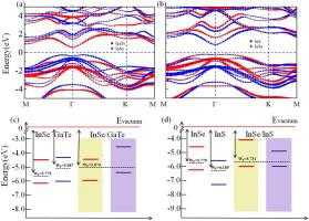
Abstract The two-dimensional (2D) group III-VI chalcogenide family is gaining growing attention due to its potential applications in future optoelectronic devices. The van der Waals (vdW) heterostructure give novel properties that do not appear in their components. Herein, by using first-principles calculations, we study the 2D InSe/GaTe and InSe/InS vdW heterostructures, considering stacking patterns, electronic structures, band alignment, in-plane and out-of-plane strains effects. Both heterostructures are indirect band gap semiconductors with gap values of 0.84 and 1.07 eV for InSe/GaTe and InSe/InS, respectively. The InSe/GaTe heterostructure possesses a typical type-II band alignment, where the electrons and holes are localized in the InSe and GaTe layers, respectively. However, the band alignment type is ambiguous for InSe/InS heterostructure because valence band maximum simultaneously contains both InSe and InS components. The application of strains can change the band alignment type and induce a semiconductor-metal transition for both heterostructures. Besides, type-II or type-I band alignment in InSe/InS heterostructure can be realized by means of external electric field. Our results suggest that the vdW heterostructures based on 2D group III–VI chalcogenide family possess the tunable band alignment and band gap, which are very significant in the optoelectronic devices.
中文翻译:

InSe/GaTe 和 InSe/InS van der Waals 异质结构中能带对齐的操纵
摘要 二维 (2D) III-VI 族硫属化物家族因其在未来光电器件中的潜在应用而受到越来越多的关注。范德华 (vdW) 异质结构提供了其组件中没有的新特性。在此,通过使用第一性原理计算,我们研究了二维 InSe/GaTe 和 InSe/InS vdW 异质结构,同时考虑了堆叠模式、电子结构、能带对齐、面内和面外应变效应。两种异质结构都是间接带隙半导体,InSe/GaTe 和 InSe/InS 的间隙值分别为 0.84 和 1.07 eV。InSe/GaTe 异质结构具有典型的 II 型能带排列,其中电子和空穴分别位于 InSe 和 GaTe 层中。然而,InSe/InS 异质结构的能带对齐类型不明确,因为价带最大值同时包含 InSe 和 InS 成分。应变的应用可以改变能带排列类型并引起两种异质结构的半导体-金属转变。此外,InSe/InS异质结构中的II型或I型能带排列可以通过外部电场实现。我们的结果表明,基于二维 III-VI 族硫族化物家族的 vdW 异质结构具有可调的带对齐和带隙,这在光电器件中非常重要。InSe/InS异质结构中的II型或I型能带排列可以通过外部电场实现。我们的结果表明,基于二维 III-VI 族硫族化物家族的 vdW 异质结构具有可调的带对齐和带隙,这在光电器件中非常重要。InSe/InS异质结构中的II型或I型能带排列可以通过外部电场实现。我们的结果表明,基于二维 III-VI 族硫族化物家族的 vdW 异质结构具有可调的带对齐和带隙,这在光电器件中非常重要。
更新日期:2021-02-01
中文翻译:
InSe/GaTe 和 InSe/InS van der Waals 异质结构中能带对齐的操纵
摘要 二维 (2D) III-VI 族硫属化物家族因其在未来光电器件中的潜在应用而受到越来越多的关注。范德华 (vdW) 异质结构提供了其组件中没有的新特性。在此,通过使用第一性原理计算,我们研究了二维 InSe/GaTe 和 InSe/InS vdW 异质结构,同时考虑了堆叠模式、电子结构、能带对齐、面内和面外应变效应。两种异质结构都是间接带隙半导体,InSe/GaTe 和 InSe/InS 的间隙值分别为 0.84 和 1.07 eV。InSe/GaTe 异质结构具有典型的 II 型能带排列,其中电子和空穴分别位于 InSe 和 GaTe 层中。然而,InSe/InS 异质结构的能带对齐类型不明确,因为价带最大值同时包含 InSe 和 InS 成分。应变的应用可以改变能带排列类型并引起两种异质结构的半导体-金属转变。此外,InSe/InS异质结构中的II型或I型能带排列可以通过外部电场实现。我们的结果表明,基于二维 III-VI 族硫族化物家族的 vdW 异质结构具有可调的带对齐和带隙,这在光电器件中非常重要。InSe/InS异质结构中的II型或I型能带排列可以通过外部电场实现。我们的结果表明,基于二维 III-VI 族硫族化物家族的 vdW 异质结构具有可调的带对齐和带隙,这在光电器件中非常重要。InSe/InS异质结构中的II型或I型能带排列可以通过外部电场实现。我们的结果表明,基于二维 III-VI 族硫族化物家族的 vdW 异质结构具有可调的带对齐和带隙,这在光电器件中非常重要。


 京公网安备 11010802027423号