当前位置:
X-MOL 学术
›
CrystEngComm
›
论文详情
Our official English website, www.x-mol.net, welcomes your
feedback! (Note: you will need to create a separate account there.)
An electronic phase diagram of hole-doped BiCuSeO crystals determined by transport characterization under various growth conditions
CrystEngComm ( IF 2.6 ) Pub Date : 2020-10-29 , DOI: 10.1039/d0ce01332c Lu Xu 1, 2, 3, 4, 5 , Ye-Cheng Luo 1, 2, 3, 4, 6 , Yang-Yang Lv 1, 2, 3, 4, 6 , Yan-Yan Zhang 1, 2, 3, 4, 5 , Shuang Han 1, 2, 3, 4, 6 , Shu-Hua Yao 1, 2, 3, 4, 5 , Jian Zhou 1, 2, 3, 4, 5 , Y. B. Chen 1, 2, 3, 4, 6 , Yan-Feng Chen 1, 2, 3, 4, 5
CrystEngComm ( IF 2.6 ) Pub Date : 2020-10-29 , DOI: 10.1039/d0ce01332c Lu Xu 1, 2, 3, 4, 5 , Ye-Cheng Luo 1, 2, 3, 4, 6 , Yang-Yang Lv 1, 2, 3, 4, 6 , Yan-Yan Zhang 1, 2, 3, 4, 5 , Shuang Han 1, 2, 3, 4, 6 , Shu-Hua Yao 1, 2, 3, 4, 5 , Jian Zhou 1, 2, 3, 4, 5 , Y. B. Chen 1, 2, 3, 4, 6 , Yan-Feng Chen 1, 2, 3, 4, 5
Affiliation
|
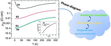
The layered compound BiCuSeO is a narrow-band-gap semiconductor that demonstrates superior thermoelectric properties. However, the electrical properties of BiCuSeO with varied hole concentrations have not been characterized systematically, and this is explored in this work. Through delicately adjusting the growth conditions via a chemical-vapor-transport method, we successfully grew a series of BiCuSeO crystals with hole-concentration (nh) values that varied from 1.0 × 10¹⁷ to 2.0 × 1020 cm−3. Our systematic characterization of electrical properties shows that when nh is around 1.0 × 1017 cm−3, BiCuSeO is an Anderson insulator when the temperature (T) is lower than 50 K, and it then transitions to a degenerate semiconductor (metal-like behavior); when nh is around 3.0 × 1018 cm−3, BiCuSeO shows the features of a degenerate semiconductor at high temperature (T > 15 K), but there is non-Fermi liquid resistance features at low-temperature (T < 15 K); while when nh is higher than 2.0 × 1020 cm−3, BiCuSeO crystals show the fingerprint of a degenerate semiconductor. In the degenerate semiconductor regime, the electron–phonon interaction strength of BiCuSeO changes from 36.1 × 10⁻³ to 3.6 × 10⁻³ when nh is increased from 1.0 × 10¹⁷ to 2.0 × 1020 cm−3, which can be semi-quantitatively explained based on the enhanced screening of Coulomb interactions with an increased hole concentration. Based on these results, a temperature-hole-concentration dependent electronic phase-diagram of BiCuSeO is proposed. This work may be referenced to modify the electrical properties of layered-compounds similar to BiCuSeO.
中文翻译:

通过在各种生长条件下的传输特性确定的掺杂空穴的BiCuSeO晶体的电子相图
层状化合物BiCuSeO是一种窄带隙半导体,具有出色的热电性能。然而,BiCuSeO具有不同的空穴浓度的电学特性尚未得到系统地表征,这在这项工作中得到了探索。通过微妙调整生长条件通过化学气相传输法,我们成功地生长具有空穴浓度(一系列BiCuSeO晶体Ñ ħ)值从1.0×10改变17〜2.0×10 20厘米-3。我们对电性能的系统表征表明,当n h约为1.0×10 17 cm -3时,当温度(T)低于50 K时,BiCuSeO是安德森绝缘体,然后转变为退化的半导体(类金属行为);当n h约为3.0×10 18 cm -3时,BiCuSeO表现出在高温下(T > 15 K)退化的半导体的特征,但在低温下(T <15 K)则存在非费米液体电阻的特征。; 而当n h高于2.0×10 20 cm -3时BiCuSeO晶体显示了退化的半导体的指纹。在简并半导体制度,BiCuSeO的电子-声子的相互作用强度改变从36.1×10 -3至3.6×10 -3时ñ ħ从1.0×10增加到17〜2.0×10 20厘米-3,其可以是半-基于对库仑相互作用的增强筛选和增加的空穴浓度来定量解释。基于这些结果,提出了BiCuSeO的温度-孔浓度依赖性电子相图。可以参考这项工作来修改类似于BiCuSeO的层状化合物的电性能。
更新日期:2020-11-15
中文翻译:
通过在各种生长条件下的传输特性确定的掺杂空穴的BiCuSeO晶体的电子相图
层状化合物BiCuSeO是一种窄带隙半导体,具有出色的热电性能。然而,BiCuSeO具有不同的空穴浓度的电学特性尚未得到系统地表征,这在这项工作中得到了探索。通过微妙调整生长条件通过化学气相传输法,我们成功地生长具有空穴浓度(一系列BiCuSeO晶体Ñ ħ)值从1.0×10改变17〜2.0×10 20厘米-3。我们对电性能的系统表征表明,当n h约为1.0×10 17 cm -3时,当温度(T)低于50 K时,BiCuSeO是安德森绝缘体,然后转变为退化的半导体(类金属行为);当n h约为3.0×10 18 cm -3时,BiCuSeO表现出在高温下(T > 15 K)退化的半导体的特征,但在低温下(T <15 K)则存在非费米液体电阻的特征。; 而当n h高于2.0×10 20 cm -3时BiCuSeO晶体显示了退化的半导体的指纹。在简并半导体制度,BiCuSeO的电子-声子的相互作用强度改变从36.1×10 -3至3.6×10 -3时ñ ħ从1.0×10增加到17〜2.0×10 20厘米-3,其可以是半-基于对库仑相互作用的增强筛选和增加的空穴浓度来定量解释。基于这些结果,提出了BiCuSeO的温度-孔浓度依赖性电子相图。可以参考这项工作来修改类似于BiCuSeO的层状化合物的电性能。


 京公网安备 11010802027423号