当前位置:
X-MOL 学术
›
Laser Photonics Rev.
›
论文详情
Our official English website, www.x-mol.net, welcomes your
feedback! (Note: you will need to create a separate account there.)
Hybrid/Integrated Silicon Photonics Based on 2D Materials in Optical Communication Nanosystems
Laser & Photonics Reviews ( IF 9.8 ) Pub Date : 2020-11-12 , DOI: 10.1002/lpor.202000239 Jie You 1 , Yukun Luo 1 , Jie Yang 1 , Jianghua Zhang 1 , Ke Yin 1 , Ke Wei 2 , Xin Zheng 1 , Tian Jiang 2
Laser & Photonics Reviews ( IF 9.8 ) Pub Date : 2020-11-12 , DOI: 10.1002/lpor.202000239 Jie You 1 , Yukun Luo 1 , Jie Yang 1 , Jianghua Zhang 1 , Ke Yin 1 , Ke Wei 2 , Xin Zheng 1 , Tian Jiang 2
Affiliation
|
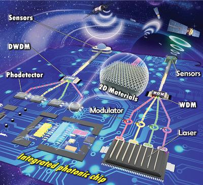
Silicon (Si) photonics have established as leading technologies in addressing the rapidly increasing demands of huge data transfer in optical communication systems with compact footprints, small power consumption, and ultradense bandwidth, which are driven by the next generation supercomputers and big data era. Particularly, Si photonics will penetrate into optical communication links at an ever‐small scale, namely chip‐to‐chip and on‐chip. However, the nanostructures made of Si with an indirect bandgap are not ideal candidates for on‐chip light sources, modulators, and photodetectors, which most‐frequently require optical materials with direct bandgap. Thanks to the advent of graphene, transition metal dichalcogenides and other two‐dimensional (2D) materials, which can facilitate extraordinary progresses in improving device performance at the ultrathin scale, their integration with Si photonics furnishes a heterogeneous platform to construct fully functional and highly integrated photonic communication systems. In this work, the current advancements in the on‐chip applications of Si photonics‐2D materials heterostructures, inclusive of all essential chip‐scale modules and integrated circuits, as well as the future prospective and challenges are reviewed and discussed. The present study sets out to objectively measure the feasibility of the hybrid integration between Si photonics and 2D materials in on‐chip optical communications and the advanced applications beyond.
中文翻译:

光通信纳米系统中基于二维材料的混合/集成硅光子学
硅(Si)光子学已成为领先技术,可解决由下一代超级计算机和大数据时代驱动的,占地面积小,功耗小和超密集带宽的光通信系统中海量数据传输的快速增长的需求。特别是,硅光子学将以很小的规模渗透到光通信链路中,即芯片到芯片和芯片上。但是,具有间接带隙的Si制成的纳米结构并不是片上光源,调制器和光电探测器的理想选择,因为片上光源,调制器和光电检测器通常需要具有直接带隙的光学材料。得益于石墨烯,过渡金属二卤化物和其他二维(2D)材料的出现,它们可以促进在超薄规模上提高器件性能的非凡进步,它们与Si光子学的集成提供了一个异构平台来构建功能齐全且高度集成的光子通信系统。在这项工作中,对Si光子2D材料异质结构在片上应用的当前进展(包括所有必不可少的芯片级模块和集成电路)以及未来的前景和挑战进行了回顾和讨论。本研究着手客观地测量Si光子学与2D材料在片上光通信中以及以后的高级应用中进行混合集成的可行性。它们与Si光子学的集成为构建功能齐全且高度集成的光子通信系统提供了一个异构平台。在这项工作中,对Si光子2D材料异质结构在片上应用的当前进展(包括所有必不可少的芯片级模块和集成电路)以及未来的前景和挑战进行了回顾和讨论。本研究着手客观地测量Si光子学与2D材料在片上光通信中以及以后的高级应用中进行混合集成的可行性。它们与Si光子学的集成为构建功能齐全且高度集成的光子通信系统提供了一个异构平台。在这项工作中,对Si光子2D材料异质结构在片上应用的当前进展(包括所有必不可少的芯片级模块和集成电路)以及未来的前景和挑战进行了回顾和讨论。本研究着手客观地测量Si光子学与2D材料在片上光通信中以及以后的高级应用中进行混合集成的可行性。以及未来的前景和挑战进行了审查和讨论。本研究着手客观地测量Si光子学与2D材料在片上光通信中以及以后的高级应用中进行混合集成的可行性。以及未来的前景和挑战进行了审查和讨论。本研究着手客观地测量Si光子学与2D材料在片上光通信中以及以后的高级应用中进行混合集成的可行性。
更新日期:2020-12-12
中文翻译:
光通信纳米系统中基于二维材料的混合/集成硅光子学
硅(Si)光子学已成为领先技术,可解决由下一代超级计算机和大数据时代驱动的,占地面积小,功耗小和超密集带宽的光通信系统中海量数据传输的快速增长的需求。特别是,硅光子学将以很小的规模渗透到光通信链路中,即芯片到芯片和芯片上。但是,具有间接带隙的Si制成的纳米结构并不是片上光源,调制器和光电探测器的理想选择,因为片上光源,调制器和光电检测器通常需要具有直接带隙的光学材料。得益于石墨烯,过渡金属二卤化物和其他二维(2D)材料的出现,它们可以促进在超薄规模上提高器件性能的非凡进步,它们与Si光子学的集成提供了一个异构平台来构建功能齐全且高度集成的光子通信系统。在这项工作中,对Si光子2D材料异质结构在片上应用的当前进展(包括所有必不可少的芯片级模块和集成电路)以及未来的前景和挑战进行了回顾和讨论。本研究着手客观地测量Si光子学与2D材料在片上光通信中以及以后的高级应用中进行混合集成的可行性。它们与Si光子学的集成为构建功能齐全且高度集成的光子通信系统提供了一个异构平台。在这项工作中,对Si光子2D材料异质结构在片上应用的当前进展(包括所有必不可少的芯片级模块和集成电路)以及未来的前景和挑战进行了回顾和讨论。本研究着手客观地测量Si光子学与2D材料在片上光通信中以及以后的高级应用中进行混合集成的可行性。它们与Si光子学的集成为构建功能齐全且高度集成的光子通信系统提供了一个异构平台。在这项工作中,对Si光子2D材料异质结构在片上应用的当前进展(包括所有必不可少的芯片级模块和集成电路)以及未来的前景和挑战进行了回顾和讨论。本研究着手客观地测量Si光子学与2D材料在片上光通信中以及以后的高级应用中进行混合集成的可行性。以及未来的前景和挑战进行了审查和讨论。本研究着手客观地测量Si光子学与2D材料在片上光通信中以及以后的高级应用中进行混合集成的可行性。以及未来的前景和挑战进行了审查和讨论。本研究着手客观地测量Si光子学与2D材料在片上光通信中以及以后的高级应用中进行混合集成的可行性。


 京公网安备 11010802027423号