当前位置:
X-MOL 学术
›
ACS Appl. Nano Mater.
›
论文详情
Our official English website, www.x-mol.net, welcomes your
feedback! (Note: you will need to create a separate account there.)
Strain-Induced Photocurrent Enhancement in Photodetectors Based on Nanometer-Thick ZnO Films on Flexible Polydimethylsiloxane Substrates
ACS Applied Nano Materials ( IF 5.3 ) Pub Date : 2020-11-09 , DOI: 10.1021/acsanm.0c02181 Jeong Heum Mun 1 , HanJin Lee 1 , Sun Hee Lee 2 , Tae-Sik Yoon 1 , Seung Ho Han 2 , Dong Hun Kim 1
ACS Applied Nano Materials ( IF 5.3 ) Pub Date : 2020-11-09 , DOI: 10.1021/acsanm.0c02181 Jeong Heum Mun 1 , HanJin Lee 1 , Sun Hee Lee 2 , Tae-Sik Yoon 1 , Seung Ho Han 2 , Dong Hun Kim 1
Affiliation
|
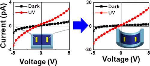
Strain-induced modulation of electronic, magnetic, and photonic properties provides additional functionalities to oxide thin film-based electronics as compared to those of conventional rigid electronics. Herein, we introduce a simple transfer process for highly crystalline nanometer-thick films onto flexible polydimethylsiloxane (PDMS) using water-soluble sacrificial NaCl crystals. The c axis of the high-temperature sputtered ZnO thin films grew along a parallel direction to the substrate surface, thereby revealing the (100) reflection on both Si and NaCl substrates, which is desirable for designing photoconductors with a planar geometry. However, films grown at room temperature showed a preferred growth orientation along the vertical direction to the substrate surface. The photodetectors synthesized using ZnO thin films grown directly on PDMS at room temperature exhibited a low current, whereas the photodetectors fabricated using ZnO thin films grown at a high temperature exhibited dramatically increased currents in the dark and under ultraviolet (UV) light. The photodetector performance was further enhanced under external strain due to the piezophototronic effect induced by bending or stretching the photodetectors under UV light. These properties were confirmed by the absorption or desorption of oxygen on the ZnO surface under the applied strains. The proposed strain-induced optoelectronic property modulation of highly crystalline ZnO thin films is promising for the development of future multifunctional flexible, transparent, and wearable electronics.
中文翻译:

柔性聚二甲基硅氧烷衬底上基于纳米厚ZnO薄膜的光电探测器中的应变诱导光电流增强
与传统的刚性电子设备相比,应变诱导的电子,磁和光子特性的调制为基于氧化物薄膜的电子设备提供了额外的功能。在这里,我们介绍了一种使用水溶性牺牲NaCl晶体将高结晶纳米厚度薄膜转移到柔性聚二甲基硅氧烷(PDMS)上的简单转移方法。该ç高温溅射ZnO薄膜的X轴沿平行于基板表面的方向生长,从而揭示了在Si和NaCl基板上的(100)反射,这对于设计具有平面几何形状的光电导体是理想的。然而,在室温下生长的膜表现出沿垂直于基材表面的垂直方向的优选生长取向。使用在室温下直接在PDMS上生长的ZnO薄膜合成的光电检测器显示出低电流,而使用在高温下生长的ZnO薄膜制造的光电检测器在黑暗和紫外(UV)光下显示出显着增加的电流。由于在紫外线下弯曲或拉伸光电探测器而产生的压电效应,在外部应变下光电探测器的性能进一步提高。在施加的应变下,ZnO表面上的氧气吸收或解吸证实了这些性质。拟议的应变诱导的高度结晶的ZnO薄膜的光电特性调制对于未来多功能,灵活,透明和可穿戴的电子产品的发展是有希望的。
更新日期:2020-11-25
中文翻译:
柔性聚二甲基硅氧烷衬底上基于纳米厚ZnO薄膜的光电探测器中的应变诱导光电流增强
与传统的刚性电子设备相比,应变诱导的电子,磁和光子特性的调制为基于氧化物薄膜的电子设备提供了额外的功能。在这里,我们介绍了一种使用水溶性牺牲NaCl晶体将高结晶纳米厚度薄膜转移到柔性聚二甲基硅氧烷(PDMS)上的简单转移方法。该ç高温溅射ZnO薄膜的X轴沿平行于基板表面的方向生长,从而揭示了在Si和NaCl基板上的(100)反射,这对于设计具有平面几何形状的光电导体是理想的。然而,在室温下生长的膜表现出沿垂直于基材表面的垂直方向的优选生长取向。使用在室温下直接在PDMS上生长的ZnO薄膜合成的光电检测器显示出低电流,而使用在高温下生长的ZnO薄膜制造的光电检测器在黑暗和紫外(UV)光下显示出显着增加的电流。由于在紫外线下弯曲或拉伸光电探测器而产生的压电效应,在外部应变下光电探测器的性能进一步提高。在施加的应变下,ZnO表面上的氧气吸收或解吸证实了这些性质。拟议的应变诱导的高度结晶的ZnO薄膜的光电特性调制对于未来多功能,灵活,透明和可穿戴的电子产品的发展是有希望的。


 京公网安备 11010802027423号