当前位置:
X-MOL 学术
›
Microelectron. Eng.
›
论文详情
Our official English website, www.x-mol.net, welcomes your
feedback! (Note: you will need to create a separate account there.)
Experimental and computational investigation of low temperature Cu Sn solid-state-diffusion bonding for 3D integration
Microelectronic Engineering ( IF 2.6 ) Pub Date : 2021-02-01 , DOI: 10.1016/j.mee.2020.111479 Jian Cai , Junqiang Wang , Qian Wang
Microelectronic Engineering ( IF 2.6 ) Pub Date : 2021-02-01 , DOI: 10.1016/j.mee.2020.111479 Jian Cai , Junqiang Wang , Qian Wang
|
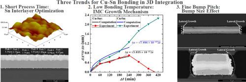
Abstract Three critical experiments, including Sn interlayer thickness optimization, interfacial IMC growth evolution, and bump size effect, have been conducted for low temperature Cu Sn solid-state-diffusion (SSD) bonding. The minimum thickness of Sn interlayer was firstly optimized to shorten the bonding time through surface and interface analysis. During bonding and annealing processes for sandwich-structured Cu/Sn/Cu interconnection, Sn interlayer exhausting and intermetallic compounds (IMCs) transforming were then investigated detailly. The growth mechanism of Cu6Sn5 and Cu3Sn in low temperature Cu Sn bonding was still controlled by lattice diffusion. However, Cu6Sn5 growth inhibited Cu3Sn growth when Sn existed. Finally, a stable three-layer structure of Cu/Cu3Sn/Cu could form at bonding interface. Also, bump size effect due to IMC lateral growth have been demonstrated for fine-pitch interconnection. It is concluded these investigations would facilitate the application of low temperature Cu Sn SSD bonding for high-density 3D integration.
中文翻译:

用于 3D 集成的低温 Cu Sn 固态扩散键合的实验和计算研究
摘要 对低温Cu Sn 固态扩散(SSD) 键合进行了三个关键实验,包括Sn 层间厚度优化、界面IMC 生长演变和凸块尺寸效应。首先通过表面和界面分析优化Sn中间层的最小厚度以缩短键合时间。在夹层结构的 Cu/Sn/Cu 互连的键合和退火过程中,详细研究了 Sn 层间排放和金属间化合物 (IMC) 转变。Cu6Sn5和Cu3Sn在低温Cu Sn键合中的生长机制仍受晶格扩散控制。然而,当 Sn 存在时,Cu6Sn5 的生长会抑制 Cu3Sn 的生长。最后,可以在键合界面形成稳定的 Cu/Cu3Sn/Cu 三层结构。还,由于 IMC 横向生长导致的凸块尺寸效应已被证明用于细间距互连。得出的结论是,这些研究将促进低温 Cu Sn SSD 键合在高密度 3D 集成中的应用。
更新日期:2021-02-01
中文翻译:
用于 3D 集成的低温 Cu Sn 固态扩散键合的实验和计算研究
摘要 对低温Cu Sn 固态扩散(SSD) 键合进行了三个关键实验,包括Sn 层间厚度优化、界面IMC 生长演变和凸块尺寸效应。首先通过表面和界面分析优化Sn中间层的最小厚度以缩短键合时间。在夹层结构的 Cu/Sn/Cu 互连的键合和退火过程中,详细研究了 Sn 层间排放和金属间化合物 (IMC) 转变。Cu6Sn5和Cu3Sn在低温Cu Sn键合中的生长机制仍受晶格扩散控制。然而,当 Sn 存在时,Cu6Sn5 的生长会抑制 Cu3Sn 的生长。最后,可以在键合界面形成稳定的 Cu/Cu3Sn/Cu 三层结构。还,由于 IMC 横向生长导致的凸块尺寸效应已被证明用于细间距互连。得出的结论是,这些研究将促进低温 Cu Sn SSD 键合在高密度 3D 集成中的应用。


 京公网安备 11010802027423号