当前位置:
X-MOL 学术
›
Microelectron. Eng.
›
论文详情
Our official English website, www.x-mol.net, welcomes your
feedback! (Note: you will need to create a separate account there.)
Characterization of silane based ultra-thin barrier deposited at elevated temperature
Microelectronic Engineering ( IF 2.6 ) Pub Date : 2021-01-01 , DOI: 10.1016/j.mee.2020.111468 Kian Kadan-Jamal , Rakefet Ofek Almog , Junyi Zhou , Tali Dotan , Yelena Sverdlov , Ronen Dagan , Yosi Shacham-Diamand
Microelectronic Engineering ( IF 2.6 ) Pub Date : 2021-01-01 , DOI: 10.1016/j.mee.2020.111468 Kian Kadan-Jamal , Rakefet Ofek Almog , Junyi Zhou , Tali Dotan , Yelena Sverdlov , Ronen Dagan , Yosi Shacham-Diamand
|
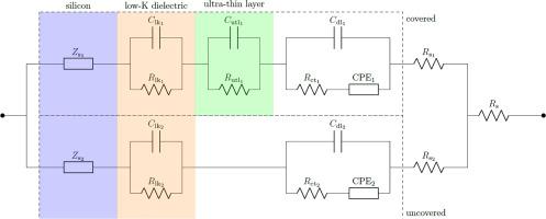
Abstract In this work, we describe a quick turn-around characterization approach of ultra-thin layers on low dielectric constant (Low-K) interlevel dielectric using Electrochemical Impedance Spectroscopy (EIS). It is demonstrated on an organo-silane based ultra-thin Cu barrier layer, deposited from liquid phase at elevated temperatures, 90 °C - 150 °C, using high flash temperature solvents: N-methyl-2-pyrrolydone (NMP, Tflash-point = 91 °C) or Ethylene glycol (EG, Tflash-point = 116 °C). Three Silane (Head group) based monomers; with three different tail groups (e.g. amine, aniline and methacrylate) were investigated; The elevated temperature deposition process allowed shorter deposition times (less than 15 min), compared to previous publications. Additionally, the high flash point solvents reduce the risk of spontaneous explosion or ignition. All three monomers yielded satisfactory barrier against copper transport, being tested for more than 10 h at temperature higher than 400 °C, on all substrates. The need for a quick turn-around and a simple way to determine the barrier presence, its thickness and its coverage, lead to explore the application of Electrochemical Impedance Spectroscopy (EIS). We demonstrate the capability of that method estimating thickness and coverage of such ultra-thin barriers deposited on relatively thick (~200 nm) Low-K dielectric materials. It was found that EIS below 10 Hz at negative wafer bias vs. the electrolyte reference, the impedance real part was affected by the ultra-thin layer on thick dielectric materials allowing to define an Effective Electrical Coverage (EEC) of the films on Low-K dielectric similar to what has already been defined on bare silicon. The EEC is a figure of merit and its relation to the actual surface coverage, and barrier properties, is briefly discussed.
中文翻译:

在高温下沉积的硅烷基超薄阻挡层的表征
摘要 在这项工作中,我们描述了一种使用电化学阻抗谱 (EIS) 对低介电常数 (Low-K) 层间电介质上的超薄层进行快速周转表征的方法。它在有机硅烷基超薄铜阻挡层上得到证明,该层在 90 °C - 150 °C 的高温下从液相沉积,使用高闪点温度溶剂:N-甲基-2-吡咯烷酮(NMP、Tflash点 = 91 °C)或乙二醇(EG,T 闪点 = 116 °C)。三硅烷(首基)基单体;研究了三个不同的尾基(例如胺、苯胺和甲基丙烯酸酯);与以前的出版物相比,高温沉积过程允许更短的沉积时间(小于 15 分钟)。此外,高闪点溶剂可降低自爆或着火的风险。在高于 400 °C 的温度下,在所有基材上测试了超过 10 小时,所有三种单体都对铜传输产生了令人满意的阻隔。需要快速周转和确定屏障存在、其厚度和覆盖范围的简单方法,导致探索电化学阻抗谱 (EIS) 的应用。我们展示了该方法估计沉积在相对厚 (~200 nm) 低 K 介电材料上的这种超薄势垒的厚度和覆盖率的能力。发现在负晶片偏压下 EIS 低于 10 Hz,与电解质参考相比,阻抗实部受厚介电材料上超薄层的影响,允许在低 K 介电质上定义薄膜的有效电覆盖 (EEC),类似于已在裸硅上定义的。EEC 是一个品质因数,并简要讨论了它与实际表面覆盖率和阻隔性能的关系。
更新日期:2021-01-01
中文翻译:
在高温下沉积的硅烷基超薄阻挡层的表征
摘要 在这项工作中,我们描述了一种使用电化学阻抗谱 (EIS) 对低介电常数 (Low-K) 层间电介质上的超薄层进行快速周转表征的方法。它在有机硅烷基超薄铜阻挡层上得到证明,该层在 90 °C - 150 °C 的高温下从液相沉积,使用高闪点温度溶剂:N-甲基-2-吡咯烷酮(NMP、Tflash点 = 91 °C)或乙二醇(EG,T 闪点 = 116 °C)。三硅烷(首基)基单体;研究了三个不同的尾基(例如胺、苯胺和甲基丙烯酸酯);与以前的出版物相比,高温沉积过程允许更短的沉积时间(小于 15 分钟)。此外,高闪点溶剂可降低自爆或着火的风险。在高于 400 °C 的温度下,在所有基材上测试了超过 10 小时,所有三种单体都对铜传输产生了令人满意的阻隔。需要快速周转和确定屏障存在、其厚度和覆盖范围的简单方法,导致探索电化学阻抗谱 (EIS) 的应用。我们展示了该方法估计沉积在相对厚 (~200 nm) 低 K 介电材料上的这种超薄势垒的厚度和覆盖率的能力。发现在负晶片偏压下 EIS 低于 10 Hz,与电解质参考相比,阻抗实部受厚介电材料上超薄层的影响,允许在低 K 介电质上定义薄膜的有效电覆盖 (EEC),类似于已在裸硅上定义的。EEC 是一个品质因数,并简要讨论了它与实际表面覆盖率和阻隔性能的关系。


 京公网安备 11010802027423号