当前位置:
X-MOL 学术
›
Surf. Sci.
›
论文详情
Our official English website, www.x-mol.net, welcomes your
feedback! (Note: you will need to create a separate account there.)
A New 2D Si3X(X=S, 0) Direct Band Gap Semiconductor with Anisotropic Carrier Mobility
Surface Science ( IF 2.1 ) Pub Date : 2021-02-01 , DOI: 10.1016/j.susc.2020.121736 Abdul Jalil , Syed Zafar Ilyas , Sarfraz Ahmed , Ather Hassan , Delong Li , Kevin Musselman , Qasim Khan
Surface Science ( IF 2.1 ) Pub Date : 2021-02-01 , DOI: 10.1016/j.susc.2020.121736 Abdul Jalil , Syed Zafar Ilyas , Sarfraz Ahmed , Ather Hassan , Delong Li , Kevin Musselman , Qasim Khan
|
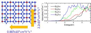
ABSTRACT Two-dimensional (2D) materials are considered to be next-generation materials due to their extraordinary electronic and optical properties. Particularly, the moderate band gap and high carrier mobility of 2D materials are highly desired for nanoelectronics applications. Herein, we explore the structural, electronic and optical properties of 2D Si3X (X=S or O) monolayers. The anisotropic monolayers are predicted to have direct bandgaps of 0.94 eV (Si3S) and 1.19 eV (Si3O) (determined using the Heyd, Scuseria, and Ernzerhof screened hybrid method) and exhibt strong optical absorption in the range of 106 cm−1. They are also predicted to have high electron and hole mobilities up to 0.5 × 103 cm2 V−1 s−1and 2.2 × 103 cm2 V−1 s−1. Due to the distinctive structural, electronic and optical properties, the 2D anisotropic Si3X monolayer is a promising material for future optoelectronic and nanoelectronic applications.
中文翻译:

具有各向异性载流子迁移率的新型二维 Si3X(X=S, 0) 直接带隙半导体
摘要 二维 (2D) 材料由于其非凡的电子和光学特性而被认为是下一代材料。特别是,二维材料的适中带隙和高载流子迁移率对于纳米电子应用是非常需要的。在此,我们探索了 2D Si3X(X=S 或 O)单层的结构、电子和光学特性。预计各向异性单层具有 0.94 eV (Si3S) 和 1.19 eV (Si3O) 的直接带隙(使用 Heyd、Scuseria 和 Ernzerhof 筛选混合方法确定),并在 106 cm-1 范围内表现出强光吸收。预计它们还具有高达 0.5 × 103 cm2 V−1 s−1 和 2.2 × 103 cm2 V−1 s−1 的高电子和空穴迁移率。由于其独特的结构、电子和光学特性,
更新日期:2021-02-01
中文翻译:
具有各向异性载流子迁移率的新型二维 Si3X(X=S, 0) 直接带隙半导体
摘要 二维 (2D) 材料由于其非凡的电子和光学特性而被认为是下一代材料。特别是,二维材料的适中带隙和高载流子迁移率对于纳米电子应用是非常需要的。在此,我们探索了 2D Si3X(X=S 或 O)单层的结构、电子和光学特性。预计各向异性单层具有 0.94 eV (Si3S) 和 1.19 eV (Si3O) 的直接带隙(使用 Heyd、Scuseria 和 Ernzerhof 筛选混合方法确定),并在 106 cm-1 范围内表现出强光吸收。预计它们还具有高达 0.5 × 103 cm2 V−1 s−1 和 2.2 × 103 cm2 V−1 s−1 的高电子和空穴迁移率。由于其独特的结构、电子和光学特性,


 京公网安备 11010802027423号