当前位置:
X-MOL 学术
›
Curr. Appl. Phys.
›
论文详情
Our official English website, www.x-mol.net, welcomes your
feedback! (Note: you will need to create a separate account there.)
Mapping of the Electronic Work Function Anisotropy of RF Sputtered Molybdenum Thin Film Electrodes for Piezoelectric Devices
Current Applied Physics ( IF 2.4 ) Pub Date : 2021-01-01 , DOI: 10.1016/j.cap.2020.10.010 Neha Sharma , Ravi Kumar , J. Jayabalan
Current Applied Physics ( IF 2.4 ) Pub Date : 2021-01-01 , DOI: 10.1016/j.cap.2020.10.010 Neha Sharma , Ravi Kumar , J. Jayabalan
|
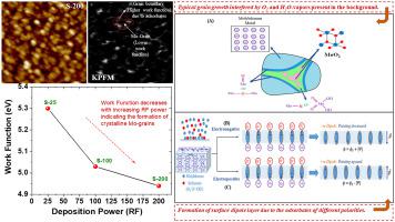
Abstract Amplitude modulated Kelvin probe force microscopy was performed on molybdenum (Mo)-thin films deposited on Si(001) substrates by RF magnetron sputtering. Evolution of film microstructure from amorphous to crystalline was observed with increasing RF power from 25 W to 200 W. Spatial mapping of work function across the film surface revealed that the Mo-thin film deposited at 200 W possesses an average work function ∼4.94 ± 0.06 eV while higher values were observed at lower RF powers. The genesis of distinct periodic changes in work function is attributed to the formation of the surface dipole layer associated with the adsorbates of different polarities (O2-/OH- or H+). A phenomenological model is also presented to elucidate their effect.
中文翻译:

用于压电器件的射频溅射钼薄膜电极的电子功函数各向异性的映射
摘要 对通过射频磁控溅射沉积在 Si(001) 衬底上的钼 (Mo) 薄膜进行了调幅开尔文探针力显微镜检查。随着射频功率从 25 W 增加到 200 W,观察到薄膜微观结构从非晶态到结晶态的演变。 薄膜表面功函数的空间映射表明,以 200 W 沉积的 Mo 薄膜具有平均功函数 ~4.94 ± 0.06 eV 而在较低的射频功率下观察到较高的值。功函数明显周期性变化的起源归因于与不同极性(O2-/OH- 或 H+)吸附物相关的表面偶极子层的形成。还提出了一个现象学模型来阐明它们的作用。
更新日期:2021-01-01
中文翻译:
用于压电器件的射频溅射钼薄膜电极的电子功函数各向异性的映射
摘要 对通过射频磁控溅射沉积在 Si(001) 衬底上的钼 (Mo) 薄膜进行了调幅开尔文探针力显微镜检查。随着射频功率从 25 W 增加到 200 W,观察到薄膜微观结构从非晶态到结晶态的演变。 薄膜表面功函数的空间映射表明,以 200 W 沉积的 Mo 薄膜具有平均功函数 ~4.94 ± 0.06 eV 而在较低的射频功率下观察到较高的值。功函数明显周期性变化的起源归因于与不同极性(O2-/OH- 或 H+)吸附物相关的表面偶极子层的形成。还提出了一个现象学模型来阐明它们的作用。


 京公网安备 11010802027423号