当前位置:
X-MOL 学术
›
Adv. Mater.
›
论文详情
Our official English website, www.x-mol.net, welcomes your
feedback! (Note: you will need to create a separate account there.)
Photonic Fractal Metamaterials: A Metal–Semiconductor Platform with Enhanced Volatile‐Compound Sensing Performance
Advanced Materials ( IF 27.4 ) Pub Date : 2020-10-22 , DOI: 10.1002/adma.202002471 Zelio Fusco 1 , Mohsen Rahmani 2 , Thanh Tran‐Phu 1 , Chiara Ricci 1 , Alexander Kiy 3 , Patrick Kluth 3 , Enrico Della Gaspera 4 , Nunzio Motta 5 , Dragomir Neshev 6 , Antonio Tricoli 1
Advanced Materials ( IF 27.4 ) Pub Date : 2020-10-22 , DOI: 10.1002/adma.202002471 Zelio Fusco 1 , Mohsen Rahmani 2 , Thanh Tran‐Phu 1 , Chiara Ricci 1 , Alexander Kiy 3 , Patrick Kluth 3 , Enrico Della Gaspera 4 , Nunzio Motta 5 , Dragomir Neshev 6 , Antonio Tricoli 1
Affiliation
|
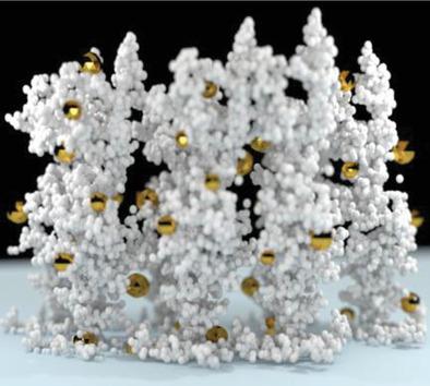
Advance of photonics media is restrained by the lack of structuring techniques for the 3D fabrication of active materials with long‐range periodicity. A methodology is reported for the engineering of tunable resonant photonic media with thickness exceeding the plasmonic near‐field enhancement region by more than two orders of magnitude. The media architecture consists of a stochastically ordered distribution of plasmonic nanocrystals in a fractal scaffold of high‐index semiconductors. This plasmonic‐semiconductor fractal media supports the propagation of surface plasmons with drastically enhanced intensity over multiple length scales, overcoming the 2D limitations of established metasurface technologies. The fractal media are used for the fabrication of plasmonic optical gas sensors, achieving a limit of detection of 0.01 vol% at room temperature and sensitivity up to 1.9 nm vol%−1, demonstrating almost a fivefold increase with respect to an optimized planar geometry. Beneficially to their implementation, the self‐assembly mechanism of this fractal architecture allows fabrication of micrometer‐thick media over surfaces of several square centimeters in a few seconds. The designable optical features and intrinsic scalability of these photonic fractal metamaterials provide ample opportunities for applications, bridging across transformation optics, sensing, and light harvesting.
中文翻译:

光子分形超材料:具有增强的挥发性化合物传感性能的金属半导体平台
光子学介质的发展受到用于长期周期性活性材料3D制造的结构化技术的限制。据报道,一种可调谐共振光子介质的工程设计方法,其厚度超过等离子体近场增强区域的幅度超过了两个数量级。介质结构由高折射率半导体的分形支架中的等离子体纳米晶体的随机有序分布组成。这种等离子体半导体分形介质支持表面等离子体激元在多个长度尺度上的传播,其强度大大增强,克服了已建立的超表面技术的二维局限性。分形介质用于制造等离激元光学气体传感器,检测极限为0。-1,相对于优化的平面几何形状几乎增加了五倍。有利于其实施,这种分形架构的自组装机制允许在几秒钟内在几平方厘米的表面上制造微米级的介质。这些光子分形超材料的可设计光学特征和内在可扩展性为应用提供了充足的机会,跨越了转换光学,传感和光收集之间的桥梁。
更新日期:2020-12-15
中文翻译:
光子分形超材料:具有增强的挥发性化合物传感性能的金属半导体平台
光子学介质的发展受到用于长期周期性活性材料3D制造的结构化技术的限制。据报道,一种可调谐共振光子介质的工程设计方法,其厚度超过等离子体近场增强区域的幅度超过了两个数量级。介质结构由高折射率半导体的分形支架中的等离子体纳米晶体的随机有序分布组成。这种等离子体半导体分形介质支持表面等离子体激元在多个长度尺度上的传播,其强度大大增强,克服了已建立的超表面技术的二维局限性。分形介质用于制造等离激元光学气体传感器,检测极限为0。-1,相对于优化的平面几何形状几乎增加了五倍。有利于其实施,这种分形架构的自组装机制允许在几秒钟内在几平方厘米的表面上制造微米级的介质。这些光子分形超材料的可设计光学特征和内在可扩展性为应用提供了充足的机会,跨越了转换光学,传感和光收集之间的桥梁。


 京公网安备 11010802027423号