Our official English website, www.x-mol.net, welcomes your
feedback! (Note: you will need to create a separate account there.)
Toward Stable Solution-Processed High-Mobility p-Type Thin Film Transistors Based on Halide Perovskites
ACS Nano ( IF 15.8 ) Pub Date : 2020-10-20 , DOI: 10.1021/acsnano.0c02862 Santanu Jana 1 , Emanuel Carlos 1 , Shrabani Panigrahi 1 , Rodrigo Martins 1 , Elvira Fortunato 1
ACS Nano ( IF 15.8 ) Pub Date : 2020-10-20 , DOI: 10.1021/acsnano.0c02862 Santanu Jana 1 , Emanuel Carlos 1 , Shrabani Panigrahi 1 , Rodrigo Martins 1 , Elvira Fortunato 1
Affiliation
|
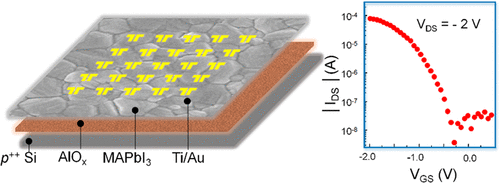
Organolead halide perovskites have drawn significant attention from the scientific community as one of the most attractive materials in optoelectronics, especially in the field of photovoltaics. In this study, we focus on using halide perovskites in processing thin film transistors (TFTs). Halide perovskites have high solution processability and excellent carrier transport characteristics, in particular for holes. The present work aims to fill a gap in oxide-based technology. It concerns the process of using high-stable and reliable p-type oxide-based devices to target CMOS technology (complementary metal-oxide-semiconductor). We report on a solution-processed high-performance TFT based on methylammonium lead iodide (CH3NH3PbI3) perovskite semiconductor films, which shows promise for devices that can be simple to manufacture with high reliability, reproducibility, and excellent stability in atmospheric conditions. To achieve a highly stable perovskite semiconductor film, we introduce diethylsulfide in the perovskite precursor. The TFT shows a stable p-type behavior when operated at low voltages (≤−2 V) and has a current modulation of >104, an almost negligible hysteresis, and average saturation mobility of about 18.8 cm2 V–1 s–1, taken over 50 devices tested (the highest one measured was ∼23.2 cm2 V–1 s–1). This is the highest value until now reported in the literature. In addition, we demonstrate that perovskite TFTs can be fabricated at temperatures as low as 150 °C on flexible substrates with a saturation mobility of ∼11.5 cm2 V–1 s–1. The high-performance perovskite TFT with excellent stability is a promising candidate for the next generation of p-type transistors for a plethora of low-cost electronics applications.
中文翻译:

走向稳定的溶液加工高迁移率μ -型薄膜晶体管基于在卤化钙钛矿
作为有机光电子中最有吸引力的材料之一,有机油卤化物钙钛矿已经引起了科学界的极大关注,特别是在光伏领域。在这项研究中,我们专注于在处理薄膜晶体管(TFT)中使用卤化钙钛矿。卤化物钙钛矿具有很高的溶液加工性和出色的载流子传输特性,尤其是对于空穴而言。本工作旨在填补基于氧化物的技术的空白。它涉及使用高稳定可靠p的过程-型基于氧化物的设备到目标CMOS技术(互补金属氧化物半导体)。我们报道了一种基于甲基铵碘化铅(CH 3 NH 3 PbI 3钙钛矿半导体膜,这显示出有望在大气条件下易于制造,具有高可靠性,可重复性和出色稳定性的器件的前景。为了获得高度稳定的钙钛矿半导体膜,我们在钙钛矿前体中引入了二乙基硫。的TFT示出了稳定的p -当在低电压下(≤-2 V)操作类型的行为,并且具有的电流调制> 10 4,几乎可忽略的滞后,以及约18.8厘米平均饱和迁移率2 V -1小号-1,对50多个测试设备进行了测量(测量的最高设备约为23.2 cm 2 V –1 s –1)。这是迄今为止文献中报道的最高值。此外,我们证明钙钛矿TFT可以在低至150°C的温度下在柔性基板上制造,其迁移率约为11.5 cm 2 V –1 s –1。具有出色稳定性的高性能钙钛矿TFT是用于众多低成本电子应用的下一代p型晶体管的有希望的候选者。
更新日期:2020-11-25
中文翻译:
走向稳定的溶液加工高迁移率μ -型薄膜晶体管基于在卤化钙钛矿
作为有机光电子中最有吸引力的材料之一,有机油卤化物钙钛矿已经引起了科学界的极大关注,特别是在光伏领域。在这项研究中,我们专注于在处理薄膜晶体管(TFT)中使用卤化钙钛矿。卤化物钙钛矿具有很高的溶液加工性和出色的载流子传输特性,尤其是对于空穴而言。本工作旨在填补基于氧化物的技术的空白。它涉及使用高稳定可靠p的过程-型基于氧化物的设备到目标CMOS技术(互补金属氧化物半导体)。我们报道了一种基于甲基铵碘化铅(CH 3 NH 3 PbI 3钙钛矿半导体膜,这显示出有望在大气条件下易于制造,具有高可靠性,可重复性和出色稳定性的器件的前景。为了获得高度稳定的钙钛矿半导体膜,我们在钙钛矿前体中引入了二乙基硫。的TFT示出了稳定的p -当在低电压下(≤-2 V)操作类型的行为,并且具有的电流调制> 10 4,几乎可忽略的滞后,以及约18.8厘米平均饱和迁移率2 V -1小号-1,对50多个测试设备进行了测量(测量的最高设备约为23.2 cm 2 V –1 s –1)。这是迄今为止文献中报道的最高值。此外,我们证明钙钛矿TFT可以在低至150°C的温度下在柔性基板上制造,其迁移率约为11.5 cm 2 V –1 s –1。具有出色稳定性的高性能钙钛矿TFT是用于众多低成本电子应用的下一代p型晶体管的有希望的候选者。


 京公网安备 11010802027423号