当前位置:
X-MOL 学术
›
Appl. Surf. Sci.
›
论文详情
Our official English website, www.x-mol.net, welcomes your
feedback! (Note: you will need to create a separate account there.)
Light-assisted scanning probe microscopy characterization of the electrical properties of AlGaN/GaN/Si heterostructures
Applied Surface Science ( IF 6.3 ) Pub Date : 2021-02-01 , DOI: 10.1016/j.apsusc.2020.148189 Adam Szyszka , Mateusz Wośko , Regina Paszkiewicz
Applied Surface Science ( IF 6.3 ) Pub Date : 2021-02-01 , DOI: 10.1016/j.apsusc.2020.148189 Adam Szyszka , Mateusz Wośko , Regina Paszkiewicz
|
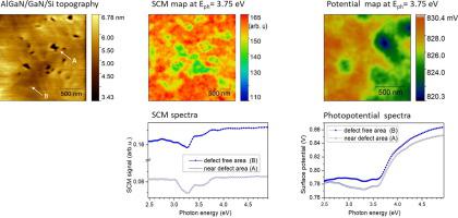
Abstract The article proposes a new methodology that combined light-assisted Scanning Surface Potential Microscopy (SSPM), Scanning Spreading Resistance Microscopy (SSRM) and Scanning Capacitance Microscopy (SCM) techniques for the extended nanoscale characterization of the electrical properties of AlGaN/GaN/Si heterostructures. Two measurement regimes were used to investigate the influence of surface defects on local electrical properties of samples: surface mapping with additional light excitation and one-point spectroscopy which enabled the accurate investigation of energetic transitions associated with a specific surface structure. The influence of two types of surface defects existing in the AlGaN/GaN/Si samples grown by metalorganic chemical vapour deposition epitaxy on the two-dimensional electron gas (2DEG) formation process on the AlGaN/GaN interface was explained. In the case of the sample with the SiN nanomasking layer added to the growth scheme, the areas of negative charge associated with defects created the localised, isolated islands that did not influence the process of electric field formation in the AlGaN/GaN system and had no significantly detrimental impact on the electron transport. The presence of surface defects in the sample without the SiN layer caused the disturbance of the 2DEG electrical properties not only in the place of the defect’s presence but also at some distance away from it. In that case, the photovoltage and photoconductivity spectra indicated the existence of a disordered structure of the AlGaN layer, near and away from the defects. Additionally, it was clarified that the characteristic electronic transition at 3.0 eV related to a deep trap state existing in the AlGaN barrier was localised solely at the surface site of the defects. It was observed during the SSRM measurements that both types of defects created a leakage current paths with prolonged conductivity (up to several seconds), which effect was not reported earlier, that provide an original insight into the origins of the long relaxation time effects existing in the AlGaN/GaN heterostructures.
中文翻译:

光辅助扫描探针显微镜表征 AlGaN/GaN/Si 异质结构的电性能
摘要 本文提出了一种结合光辅助扫描表面电位显微镜 (SSPM)、扫描扩展电阻显微镜 (SSRM) 和扫描电容显微镜 (SCM) 技术的新方法,用于对 AlGaN/GaN/Si 的电特性进行扩展纳米级表征。异质结构。两种测量方式用于研究表面缺陷对样品局部电特性的影响:具有额外光激发的表面映射和单点光谱法,能够准确研究与特定表面结构相关的能量转变。解释了金属有机化学气相沉积外延生长的AlGaN/GaN/Si样品中存在的两种表面缺陷对AlGaN/GaN界面二维电子气(2DEG)形成过程的影响。在将 SiN 纳米掩模层添加到生长方案中的样品的情况下,与缺陷相关的负电荷区域产生了局部的孤立岛,这些岛不影响 AlGaN/GaN 系统中的电场形成过程,并且没有对电子传输产生显着的不利影响。没有SiN层的样品中表面缺陷的存在不仅在缺陷存在的地方而且在远离缺陷的地方引起了2DEG电学特性的干扰。在这种情况下,光电压和光电导光谱表明,在缺陷附近和远离缺陷处,AlGaN 层存在无序结构。此外,澄清了与存在于 AlGaN 势垒中的深陷阱态相关的 3.0 eV 的特征电子跃迁仅位于缺陷的表面位置。在 SSRM 测量过程中观察到,两种类型的缺陷都会产生具有延长电导率(长达几秒)的漏电流路径,这种影响之前没有报道过,这提供了对存在于中的长弛豫时间效应起源的原始见解。 AlGaN/GaN 异质结构。与存在于 AlGaN 势垒中的深陷阱态相关的 0 eV 仅位于缺陷的表面位置。在 SSRM 测量过程中观察到,两种类型的缺陷都会产生具有延长电导率(长达几秒)的漏电流路径,这种影响之前没有报道过,这提供了对存在于中的长弛豫时间效应起源的原始见解。 AlGaN/GaN 异质结构。与存在于 AlGaN 势垒中的深陷阱态相关的 0 eV 仅位于缺陷的表面位置。在 SSRM 测量过程中观察到,两种类型的缺陷都会产生具有延长电导率(长达几秒)的漏电流路径,这种影响之前没有报道过,这提供了对存在于中的长弛豫时间效应起源的原始见解。 AlGaN/GaN 异质结构。
更新日期:2021-02-01
中文翻译:
光辅助扫描探针显微镜表征 AlGaN/GaN/Si 异质结构的电性能
摘要 本文提出了一种结合光辅助扫描表面电位显微镜 (SSPM)、扫描扩展电阻显微镜 (SSRM) 和扫描电容显微镜 (SCM) 技术的新方法,用于对 AlGaN/GaN/Si 的电特性进行扩展纳米级表征。异质结构。两种测量方式用于研究表面缺陷对样品局部电特性的影响:具有额外光激发的表面映射和单点光谱法,能够准确研究与特定表面结构相关的能量转变。解释了金属有机化学气相沉积外延生长的AlGaN/GaN/Si样品中存在的两种表面缺陷对AlGaN/GaN界面二维电子气(2DEG)形成过程的影响。在将 SiN 纳米掩模层添加到生长方案中的样品的情况下,与缺陷相关的负电荷区域产生了局部的孤立岛,这些岛不影响 AlGaN/GaN 系统中的电场形成过程,并且没有对电子传输产生显着的不利影响。没有SiN层的样品中表面缺陷的存在不仅在缺陷存在的地方而且在远离缺陷的地方引起了2DEG电学特性的干扰。在这种情况下,光电压和光电导光谱表明,在缺陷附近和远离缺陷处,AlGaN 层存在无序结构。此外,澄清了与存在于 AlGaN 势垒中的深陷阱态相关的 3.0 eV 的特征电子跃迁仅位于缺陷的表面位置。在 SSRM 测量过程中观察到,两种类型的缺陷都会产生具有延长电导率(长达几秒)的漏电流路径,这种影响之前没有报道过,这提供了对存在于中的长弛豫时间效应起源的原始见解。 AlGaN/GaN 异质结构。与存在于 AlGaN 势垒中的深陷阱态相关的 0 eV 仅位于缺陷的表面位置。在 SSRM 测量过程中观察到,两种类型的缺陷都会产生具有延长电导率(长达几秒)的漏电流路径,这种影响之前没有报道过,这提供了对存在于中的长弛豫时间效应起源的原始见解。 AlGaN/GaN 异质结构。与存在于 AlGaN 势垒中的深陷阱态相关的 0 eV 仅位于缺陷的表面位置。在 SSRM 测量过程中观察到,两种类型的缺陷都会产生具有延长电导率(长达几秒)的漏电流路径,这种影响之前没有报道过,这提供了对存在于中的长弛豫时间效应起源的原始见解。 AlGaN/GaN 异质结构。


 京公网安备 11010802027423号