当前位置:
X-MOL 学术
›
ACS Photonics
›
论文详情
Our official English website, www.x-mol.net, welcomes your
feedback! (Note: you will need to create a separate account there.)
Plasmonic-Induced Luminescence of MoSe2 Monolayers in a Scanning Tunneling Microscope
ACS Photonics ( IF 6.5 ) Pub Date : 2020-10-15 , DOI: 10.1021/acsphotonics.0c01101 Renaud Péchou 1 , Shuai Jia 2 , Joel Rigor 3 , Olivier Guillermet 1 , Grégory Seine 1 , Jun Lou 2 , Nicolas Large 3 , Adnen Mlayah 1, 4 , Roland Coratger 1
ACS Photonics ( IF 6.5 ) Pub Date : 2020-10-15 , DOI: 10.1021/acsphotonics.0c01101 Renaud Péchou 1 , Shuai Jia 2 , Joel Rigor 3 , Olivier Guillermet 1 , Grégory Seine 1 , Jun Lou 2 , Nicolas Large 3 , Adnen Mlayah 1, 4 , Roland Coratger 1
Affiliation
|
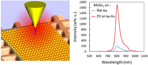
We report on a scanning tunneling microscopy-induced luminescence in MoSe2 monolayers supported by uniform and nanopatterned gold substrates. Luminescence intensity mappings, recorded with a nanometric spatial resolution, and spectroscopy measurements were performed and analyzed in terms of photon emission processes taking place within the tip–surface gap region, which supports strongly localized optical and electronic states. We found that, excited by tunneling electrons, the light emission is due to the radiative recombinations of free excitons confined within the MoSe2 monolayer. Light emission is observed at positive and negative bias voltages with very different emission rates. The results are interpreted in terms of charge carrier injection in the MoSe2 layer. Additionally, electrodynamic simulations also stress that resonance between the emitted radiation and the surface plasmons formed in the tip–surface gap region plays a critical role in the emission process. When the MoSe2 layer lays on a nanopatterned gold substrate, its luminescence intensity, induced by the tunneling electrons, is enhanced by nearly an order of magnitude. Such an effect is observed here for the first time in scanning tunneling microscopy experiments. The luminescence enhancement is attributed to the surface plasmon properties of the nanopatterned gold substrate, which spectrally match the excitonic transition of the MoSe2 layer. We show that this surface-enhanced scanning tunneling microscope-induced light emission (SESTM-LE) effect is very useful for investigating the photon emission from localized emitters (e.g., quantum wells, quantum dots, molecules) with a subnanometer spatial resolution.
中文翻译:

扫描隧道显微镜中等离子诱导的MoSe 2单层的发光。
我们报告了由均匀和纳米图案的金衬底支持的MoSe 2单层中的扫描隧道显微镜诱导的发光。进行了以纳米级空间分辨率记录的发光强度映射以及光谱测量,并根据在尖端-表面间隙区域内发生的光子发射过程进行了分析,这支持了强烈的局部光学和电子状态。我们发现,通过隧穿电子激发,光发射是由于限制在MoSe 2单层内的自由激子的辐射复合。在正和负偏置电压下观察到的光发射具有非常不同的发射速率。用MoSe 2中的载流子注入来解释结果层。此外,电动力学模拟还强调指出,发射的辐射与尖端-表面间隙区域中形成的表面等离激元之间的共振在发射过程中起着至关重要的作用。当MoSe 2层位于纳米图案的金基底上时,由隧穿电子引起的发光强度提高了近一个数量级。这种效应在扫描隧道显微镜实验中首次观察到。发光增强归因于纳米图案金基底的表面等离激元性质,该性质与MoSe 2的激子跃迁光谱匹配。层。我们表明,这种表面增强的扫描隧道显微镜诱导的光发射(SESTM-LE)效应对于研究亚纳米空间分辨率的局部发射器(例如,量子阱,量子点,分子)的光子发射非常有用。
更新日期:2020-11-18
中文翻译:
扫描隧道显微镜中等离子诱导的MoSe 2单层的发光。
我们报告了由均匀和纳米图案的金衬底支持的MoSe 2单层中的扫描隧道显微镜诱导的发光。进行了以纳米级空间分辨率记录的发光强度映射以及光谱测量,并根据在尖端-表面间隙区域内发生的光子发射过程进行了分析,这支持了强烈的局部光学和电子状态。我们发现,通过隧穿电子激发,光发射是由于限制在MoSe 2单层内的自由激子的辐射复合。在正和负偏置电压下观察到的光发射具有非常不同的发射速率。用MoSe 2中的载流子注入来解释结果层。此外,电动力学模拟还强调指出,发射的辐射与尖端-表面间隙区域中形成的表面等离激元之间的共振在发射过程中起着至关重要的作用。当MoSe 2层位于纳米图案的金基底上时,由隧穿电子引起的发光强度提高了近一个数量级。这种效应在扫描隧道显微镜实验中首次观察到。发光增强归因于纳米图案金基底的表面等离激元性质,该性质与MoSe 2的激子跃迁光谱匹配。层。我们表明,这种表面增强的扫描隧道显微镜诱导的光发射(SESTM-LE)效应对于研究亚纳米空间分辨率的局部发射器(例如,量子阱,量子点,分子)的光子发射非常有用。


 京公网安备 11010802027423号