当前位置:
X-MOL 学术
›
Appl. Surf. Sci.
›
论文详情
Our official English website, www.x-mol.net, welcomes your
feedback! (Note: you will need to create a separate account there.)
Atomic-scale silicidation of low resistivity Ni-Si system through in-situ TEM investigation
Applied Surface Science ( IF 6.3 ) Pub Date : 2021-02-01 , DOI: 10.1016/j.apsusc.2020.148129 An-Yuan Hou , Yi-Hsin Ting , Kuo-Lun Tai , Chih-Yang Huang , Kuo-Chang Lu , Wen-Wei Wu
Applied Surface Science ( IF 6.3 ) Pub Date : 2021-02-01 , DOI: 10.1016/j.apsusc.2020.148129 An-Yuan Hou , Yi-Hsin Ting , Kuo-Lun Tai , Chih-Yang Huang , Kuo-Chang Lu , Wen-Wei Wu
|
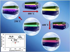
Abstract Nickel silicide has many advantages, such as low resistivity and low formation temperature; therefore, it has been widely used in the fields of solar cells, transistors and complementary metal-oxidesemiconductor (CMOS) devices. To obtain high-quality nickel-silicide thin film, solid-state reaction is a convenient and efficient fabrication method. For better understanding of the dynamic formation mechanism, we used in-situ transmission electron microscopy (TEM) to record the diffusion behavior during the heating process. In this work, three-steps annealing process to synthesize different nickel silicides corresponding to the various formation temperatures were investigated systematically. At 250 °C, the product of the first-step annealing was inverted-triangle Ni2Si, embedded in the Si substrate. Then, well-distributed NiSi thin film was synthesized, having the lowest resistivity among Ni-Si system at 400 °C. Finally, NiSi2, a Si-rich product, would form during the third-step annealing at 600 °C. NiSi2 product and Si substrate have small lattice mismatch; thus, the epitaxial relationship would be observed. We provide the evidence of diffusion behaviors and structural identification of Ni-Si system. Furthermore, these results are beneficial for the formation of specific nickel silicides, which is expected to optimize the fabrication of microelectronics.
中文翻译:

通过原位 TEM 研究低电阻率 Ni-Si 系统的原子级硅化
摘要 硅化镍具有电阻率低、形成温度低等优点。因此,它被广泛应用于太阳能电池、晶体管和互补金属氧化物半导体(CMOS)器件领域。为了获得高质量的镍硅化物薄膜,固态反应是一种方便有效的制造方法。为了更好地理解动态形成机制,我们使用原位透射电子显微镜 (TEM) 来记录加热过程中的扩散行为。在这项工作中,系统地研究了三步退火工艺以合成对应于各种形成温度的不同硅化镍。在 250 °C 时,第一步退火的产物是倒三角形 Ni2Si,嵌入在 Si 衬底中。然后,合成了分布均匀的 NiSi 薄膜,在 400 °C 时具有最低的 Ni-Si 系统电阻率。最后,在 600 °C 的第三步退火过程中会形成富含硅的 NiSi2 产品。NiSi2产物与Si衬底晶格失配小;因此,将观察到外延关系。我们提供了 Ni-Si 系统扩散行为和结构识别的证据。此外,这些结果有利于形成特定的硅化镍,有望优化微电子的制造。我们提供了 Ni-Si 系统扩散行为和结构识别的证据。此外,这些结果有利于形成特定的硅化镍,有望优化微电子的制造。我们提供了 Ni-Si 系统扩散行为和结构识别的证据。此外,这些结果有利于形成特定的硅化镍,有望优化微电子的制造。
更新日期:2021-02-01
中文翻译:
通过原位 TEM 研究低电阻率 Ni-Si 系统的原子级硅化
摘要 硅化镍具有电阻率低、形成温度低等优点。因此,它被广泛应用于太阳能电池、晶体管和互补金属氧化物半导体(CMOS)器件领域。为了获得高质量的镍硅化物薄膜,固态反应是一种方便有效的制造方法。为了更好地理解动态形成机制,我们使用原位透射电子显微镜 (TEM) 来记录加热过程中的扩散行为。在这项工作中,系统地研究了三步退火工艺以合成对应于各种形成温度的不同硅化镍。在 250 °C 时,第一步退火的产物是倒三角形 Ni2Si,嵌入在 Si 衬底中。然后,合成了分布均匀的 NiSi 薄膜,在 400 °C 时具有最低的 Ni-Si 系统电阻率。最后,在 600 °C 的第三步退火过程中会形成富含硅的 NiSi2 产品。NiSi2产物与Si衬底晶格失配小;因此,将观察到外延关系。我们提供了 Ni-Si 系统扩散行为和结构识别的证据。此外,这些结果有利于形成特定的硅化镍,有望优化微电子的制造。我们提供了 Ni-Si 系统扩散行为和结构识别的证据。此外,这些结果有利于形成特定的硅化镍,有望优化微电子的制造。我们提供了 Ni-Si 系统扩散行为和结构识别的证据。此外,这些结果有利于形成特定的硅化镍,有望优化微电子的制造。


 京公网安备 11010802027423号