当前位置:
X-MOL 学术
›
Micro Nanostruct.
›
论文详情
Our official English website, www.x-mol.net, welcomes your
feedback! (Note: you will need to create a separate account there.)
Investigation of samarium doped PbS thin films fabricated using nebulizer spray technique for photosensing applications
Micro and Nanostructures ( IF 2.7 ) Pub Date : 2020-12-01 , DOI: 10.1016/j.spmi.2020.106723 K. Paulraj , S. Ramaswamy , N. Chidhambaram , H. Algarni , Mohd Shkir , S. AlFaify
Micro and Nanostructures ( IF 2.7 ) Pub Date : 2020-12-01 , DOI: 10.1016/j.spmi.2020.106723 K. Paulraj , S. Ramaswamy , N. Chidhambaram , H. Algarni , Mohd Shkir , S. AlFaify
|
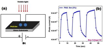
Abstract Lead sulfide (PbS) and samarium-doped (1, 3, and 5 wt%) PbS thin film layers were coated facilely on glass slides using the nebulizer spray procedure. To investigate the doping effect on the crystal structure, morphology, light absorption, and emission features of the deposited films X-ray diffraction, Raman, Scanning electron microscope, UV-Visible absorption, and photoluminescence spectroscopic analyses were carried out. A Keithley source meter was used to study the electrical characteristics of the thin film coatings. All the prepared films reveal the fcc lattice structure of PbS. Additional diffraction peaks related to the Sm2O3 phase are observed when 5wt.% of Sm was added to PbS. From Raman analysis, the peaks observed at 192, 235, and 465 cm-1 confirm the presence of the PbS phase. The scanning electron micrograph of the PbS thin film reveals that it has tightly packed grains of spherical shape. In the case of Sm doped PbS films, the mean grain size increases with the Sm doping concentration. The energy dispersive X-ray analysis shows the existence of Pb, S, and Sm which authenticates the presence of the Sm element in the PbS matrix. The optical studies reveal that the 5 wt% Sm doped PbS thin film has lower transmittance and higher absorption value. Moreover, the optical band gap value is decreased from 2.15 to 1.58 eV when Sm doping concentration increases from 0 to 5 wt%. The highest photocurrent is observed for the 3 wt.% Sm doped PbS thin film sample. The photocurrent enhancement due to the samarium doping with PbS makes it a potential candidate for the photosensor applications.
中文翻译:

使用雾化器喷雾技术制造的用于光敏应用的钐掺杂 PbS 薄膜的研究
摘要 硫化铅 (PbS) 和钐掺杂(1、3 和 5 wt%)PbS 薄膜层使用雾化器喷雾程序轻松地涂覆在载玻片上。为了研究掺杂对沉积薄膜的晶体结构、形貌、光吸收和发射特征的影响,进行了 X 射线衍射、拉曼、扫描电子显微镜、紫外-可见吸收和光致发光光谱分析。Keithley 源表用于研究薄膜涂层的电气特性。所有制备的薄膜都显示了 PbS 的 fcc 晶格结构。当 5wt.% 的 Sm 添加到 PbS 中时,观察到与 Sm2O3 相相关的额外衍射峰。根据拉曼分析,在 192、235 和 465 cm-1 处观察到的峰证实了 PbS 相的存在。PbS 薄膜的扫描电子显微照片显示它具有紧密堆积的球形颗粒。在 Sm 掺杂的 PbS 薄膜的情况下,平均晶粒尺寸随着 Sm 掺杂浓度的增加而增加。能量色散 X 射线分析显示 Pb、S 和 Sm 的存在,这证明了 PbS 矩阵中 Sm 元素的存在。光学研究表明,5 wt% Sm 掺杂的 PbS 薄膜具有较低的透射率和较高的吸收值。此外,当 Sm 掺杂浓度从 0 增加到 5 wt% 时,光学带隙值从 2.15 eV 降低到 1.58 eV。对于 3 wt.% Sm 掺杂的 PbS 薄膜样品,观察到最高的光电流。由于钐掺杂 PbS 导致的光电流增强使其成为光电传感器应用的潜在候选者。
更新日期:2020-12-01
中文翻译:
使用雾化器喷雾技术制造的用于光敏应用的钐掺杂 PbS 薄膜的研究
摘要 硫化铅 (PbS) 和钐掺杂(1、3 和 5 wt%)PbS 薄膜层使用雾化器喷雾程序轻松地涂覆在载玻片上。为了研究掺杂对沉积薄膜的晶体结构、形貌、光吸收和发射特征的影响,进行了 X 射线衍射、拉曼、扫描电子显微镜、紫外-可见吸收和光致发光光谱分析。Keithley 源表用于研究薄膜涂层的电气特性。所有制备的薄膜都显示了 PbS 的 fcc 晶格结构。当 5wt.% 的 Sm 添加到 PbS 中时,观察到与 Sm2O3 相相关的额外衍射峰。根据拉曼分析,在 192、235 和 465 cm-1 处观察到的峰证实了 PbS 相的存在。PbS 薄膜的扫描电子显微照片显示它具有紧密堆积的球形颗粒。在 Sm 掺杂的 PbS 薄膜的情况下,平均晶粒尺寸随着 Sm 掺杂浓度的增加而增加。能量色散 X 射线分析显示 Pb、S 和 Sm 的存在,这证明了 PbS 矩阵中 Sm 元素的存在。光学研究表明,5 wt% Sm 掺杂的 PbS 薄膜具有较低的透射率和较高的吸收值。此外,当 Sm 掺杂浓度从 0 增加到 5 wt% 时,光学带隙值从 2.15 eV 降低到 1.58 eV。对于 3 wt.% Sm 掺杂的 PbS 薄膜样品,观察到最高的光电流。由于钐掺杂 PbS 导致的光电流增强使其成为光电传感器应用的潜在候选者。


 京公网安备 11010802027423号