当前位置:
X-MOL 学术
›
Phys. Status Solidi. Rapid Res. Lett.
›
论文详情
Our official English website, www.x-mol.net, welcomes your
feedback! (Note: you will need to create a separate account there.)
Photosensitive Complementary Inverters Composed of n‐Channel ReS2 and p‐Channel Single‐Walled Carbon Nanotube Field‐Effect Transistors
Physica Status Solidi-Rapid Research Letters ( IF 2.5 ) Pub Date : 2020-10-06 , DOI: 10.1002/pssr.202000420 Jinheon Jeong 1 , Seung Gi Seo 1 , Seung Yeob Kim 1 , Sung Hun Jin 1
Physica Status Solidi-Rapid Research Letters ( IF 2.5 ) Pub Date : 2020-10-06 , DOI: 10.1002/pssr.202000420 Jinheon Jeong 1 , Seung Gi Seo 1 , Seung Yeob Kim 1 , Sung Hun Jin 1
Affiliation
|
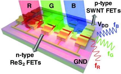
For robustness on security and ultralow power consumption for Internet of Things (IoT) sensors, including ultraminiaturization for high chip density, 2D multilayered ReS2 field‐effect transistors (FETs) combined with photoinsensitive single‐walled carbon nanotube (SWNT) FETs are demonstrated for application in light‐to‐frequency (LTF) conversion circuits. Herein, multilayered ReS2 FETs with a direct bandgap (≈1.5 eV) have discernible photoresponsivity of ≈17 A W−1 for red and ≈128 A W−1 for green, respectively, with photodetectivity (≈109 Jones), leading to excellent operation for photosensitive inverters, partly associated with the photoinsensitive SWNT FETs for p‐channel devices. Moreover, the electrical parameters for photosensitive complementary inverters, according to different wavelengths in the dark and under, red (λR = 660 nm), green (λG = 530 nm), and blue (λB = 450 nm) light, are experimentally extracted, and their SPICE simulation‐based validation on working principles of ring oscillators (ROs) is confirmed under light illumination. More impressively, ultralow power consumption for the proposed scheme is achieved due to both the direct bandgap and the large‐energy bandgap, as compared with conventional multilayered MoS2 FET‐based photosensitive inverters, rationally validating the promising opportunity for applications in the envisioned IoT sensor systems.
中文翻译:

由n通道ReS2和p通道单壁碳纳米管场效应晶体管组成的光敏互补逆变器
为了提高物联网(IoT)传感器的安全性和超低功耗的鲁棒性,包括实现高芯片密度的超小型化,将2D多层ReS 2场效应晶体管(FET)与光敏单壁碳纳米管(SWNT)FET结合使用,证明了这一点。在光频率(LTF)转换电路中的应用。在此,多层RES 2级的FET与直接带隙(≈1.5eV)的具有≈17AW的可辨别的光响应-1和用于红色≈128A,带-1为绿色,分别与photodetectivity(≈10 9琼斯(Jones),从而导致光敏逆变器的出色工作,部分与p沟道器件的光敏SWNT FET相关。此外,电气参数为感光互补反相器,根据在黑暗中和在不同的波长,红色(λ - [R = 660纳米),绿色(λ ģ = 530纳米),蓝色(λ乙 = 450nm)的光,是通过实验提取,并在光照下确认了基于SPICE仿真的环形振荡器(RO)工作原理验证。更令人印象深刻的是,与常规的多层MoS 2相比,由于直接的带隙和大的能量带隙,因此实现了拟议方案的超低功耗 基于FET的光敏逆变器,合理地验证了在设想的IoT传感器系统中应用的有前途的机会。
更新日期:2020-12-01
中文翻译:
由n通道ReS2和p通道单壁碳纳米管场效应晶体管组成的光敏互补逆变器
为了提高物联网(IoT)传感器的安全性和超低功耗的鲁棒性,包括实现高芯片密度的超小型化,将2D多层ReS 2场效应晶体管(FET)与光敏单壁碳纳米管(SWNT)FET结合使用,证明了这一点。在光频率(LTF)转换电路中的应用。在此,多层RES 2级的FET与直接带隙(≈1.5eV)的具有≈17AW的可辨别的光响应-1和用于红色≈128A,带-1为绿色,分别与photodetectivity(≈10 9琼斯(Jones),从而导致光敏逆变器的出色工作,部分与p沟道器件的光敏SWNT FET相关。此外,电气参数为感光互补反相器,根据在黑暗中和在不同的波长,红色(λ - [R = 660纳米),绿色(λ ģ = 530纳米),蓝色(λ乙 = 450nm)的光,是通过实验提取,并在光照下确认了基于SPICE仿真的环形振荡器(RO)工作原理验证。更令人印象深刻的是,与常规的多层MoS 2相比,由于直接的带隙和大的能量带隙,因此实现了拟议方案的超低功耗 基于FET的光敏逆变器,合理地验证了在设想的IoT传感器系统中应用的有前途的机会。


 京公网安备 11010802027423号