当前位置:
X-MOL 学术
›
Adv. Mater. Interfaces
›
论文详情
Our official English website, www.x-mol.net, welcomes your
feedback! (Note: you will need to create a separate account there.)
Nanoscale Mapping of Photo‐Induced Charge Carriers Generated at Interfaces of a Donor/Acceptor 2D‐Assembly by Light‐Assisted‐Scanning Tunneling Microscopy
Advanced Materials Interfaces ( IF 4.3 ) Pub Date : 2020-10-05 , DOI: 10.1002/admi.202001325 Andrés Lombana 1 , Nicolas Battaglini 1 , Samia Zrig 1 , Jérôme Lagoute 1, 2 , Alexandre Chevillot‐Biraud 1 , Philippe Lang 1
Advanced Materials Interfaces ( IF 4.3 ) Pub Date : 2020-10-05 , DOI: 10.1002/admi.202001325 Andrés Lombana 1 , Nicolas Battaglini 1 , Samia Zrig 1 , Jérôme Lagoute 1, 2 , Alexandre Chevillot‐Biraud 1 , Philippe Lang 1
Affiliation
|
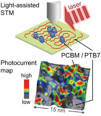
Charge transfers between donor (D) and acceptor (A) species at their excited state in a light‐assisted STM setup (LA‐STM) are investigated. Through an all‐solution process, supramolecular architectures deposited on the Au(111) surface and made of 2D islands of PC71BM (electron acceptor) on top of a single layer of the polymer PTB7 (electron donor) are elaborated. The STM junction under modulated laser irradiation exhibits a strong background of photothermal signal attributed both to vertical and lateral expansion of the tip. However, from the analysis of differential images obtained at opposite voltages, additional photocurrent peaks located at the PTB7/PC71BM interfaces are detected, providing evidence for active charge transfer between D/A species at their excited state. This phenomenon is discussed in the framework of a charge transport model at interfaces in organic electronics systems.
中文翻译:

光辅助扫描隧道显微镜在供体/受体二维组装界面上产生的光诱导载流子的纳米级映射。
在光辅助STM装置(LA-STM)中,研究了处于激发态的供体(D)和受体(A)之间的电荷转移。通过全解决方案,阐述了沉积在Au(111)表面上的超分子体系结构,该体系结构由聚合物PTB7(电子给体)单层顶部的PC 71 BM(电子受体)的2D岛制成。调制激光辐照下的STM结表现出很强的光热信号背景,这归因于尖端的垂直和横向膨胀。但是,根据对在相反电压下获得的差分图像的分析,PTB7 / PC 71处会出现其他光电流峰值检测到BM界面,为D / A物种在其激发态之间的主动电荷转移提供了证据。在有机电子系统接口处的电荷传输模型框架中讨论了这种现象。
更新日期:2020-11-21
中文翻译:
光辅助扫描隧道显微镜在供体/受体二维组装界面上产生的光诱导载流子的纳米级映射。
在光辅助STM装置(LA-STM)中,研究了处于激发态的供体(D)和受体(A)之间的电荷转移。通过全解决方案,阐述了沉积在Au(111)表面上的超分子体系结构,该体系结构由聚合物PTB7(电子给体)单层顶部的PC 71 BM(电子受体)的2D岛制成。调制激光辐照下的STM结表现出很强的光热信号背景,这归因于尖端的垂直和横向膨胀。但是,根据对在相反电压下获得的差分图像的分析,PTB7 / PC 71处会出现其他光电流峰值检测到BM界面,为D / A物种在其激发态之间的主动电荷转移提供了证据。在有机电子系统接口处的电荷传输模型框架中讨论了这种现象。


 京公网安备 11010802027423号