当前位置:
X-MOL 学术
›
Mater. Sci. Semicond. Proc.
›
论文详情
Our official English website, www.x-mol.net, welcomes your
feedback! (Note: you will need to create a separate account there.)
Selective etching of p-GaN over Al0.25Ga0.75N in Cl2/Ar/O2 ICP plasma for fabrication of normally-off GaN HEMTs
Materials Science in Semiconductor Processing ( IF 4.6 ) Pub Date : 2021-02-01 , DOI: 10.1016/j.mssp.2020.105450 Andrzej Taube , Maciej Kamiński , Marek Ekielski , Renata Kruszka , Joanna Jankowska-Śliwińska , Paweł P. Michałowski , Joanna Zdunek , Anna Szerling
Materials Science in Semiconductor Processing ( IF 4.6 ) Pub Date : 2021-02-01 , DOI: 10.1016/j.mssp.2020.105450 Andrzej Taube , Maciej Kamiński , Marek Ekielski , Renata Kruszka , Joanna Jankowska-Śliwińska , Paweł P. Michałowski , Joanna Zdunek , Anna Szerling
|
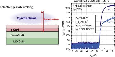
Abstract The article presents the results of development of selective etching of p-GaN over Al0.25Ga0.75N in Cl2/Ar/O2 ICP plasma for fabrication of normally-off p-GaN gate GaN HEMTs using a laser reflectometry system for precise control of the etched material thickness. By optimizing etching process parameters such as oxygen flow, ICP power and chamber pressure, high etching selectivity of p-GaN over Al0.25Ga0.75N were obtained, with values up to 56:1. High etching selectivity and the control of etch rates of p-GaN and Al0.25Ga0.75N layers withing a wide range by changing the ICP process parameters enabled application of developed etching processes in the technology of fabrication of normally-off AlGaN/GaN HEMTs with a p-GaN gate. High threshold voltage of around 1.6 V and current densities up to 400 mA/mm were obtained. Electrical measurements have shown that the shortest 1 min Al0.25Ga0.75N overetch time after selective etching of the p-GaN layer results in best electrical parameters of fabricated devices.
中文翻译:

在 Cl2/Ar/O2 ICP 等离子体中选择性蚀刻 Al0.25Ga0.75N 上的 p-GaN,用于制造常关断型 GaN HEMT
摘要 本文介绍了在 Cl2/Ar/O2 ICP 等离子体中在 Al0.25Ga0.75N 上选择性蚀刻 p-GaN 的发展结果,用于制造常关 p-GaN 栅极 GaN HEMT,使用激光反射计系统精确控制蚀刻材料的厚度。通过优化氧流量、ICP 功率和腔室压力等蚀刻工艺参数,获得了比 Al0.25Ga0.75N 更高的 p-GaN 蚀刻选择性,其值高达 56:1。高蚀刻选择性和通过改变 ICP 工艺参数在大范围内控制 p-GaN 和 Al0.25Ga0.75N 层的蚀刻速率,使已开发的蚀刻工艺能够应用于常关型 AlGaN/GaN HEMT 制造技术中p-GaN 栅极。获得了大约 1.6 V 的高阈值电压和高达 400 mA/mm 的电流密度。
更新日期:2021-02-01
中文翻译:
在 Cl2/Ar/O2 ICP 等离子体中选择性蚀刻 Al0.25Ga0.75N 上的 p-GaN,用于制造常关断型 GaN HEMT
摘要 本文介绍了在 Cl2/Ar/O2 ICP 等离子体中在 Al0.25Ga0.75N 上选择性蚀刻 p-GaN 的发展结果,用于制造常关 p-GaN 栅极 GaN HEMT,使用激光反射计系统精确控制蚀刻材料的厚度。通过优化氧流量、ICP 功率和腔室压力等蚀刻工艺参数,获得了比 Al0.25Ga0.75N 更高的 p-GaN 蚀刻选择性,其值高达 56:1。高蚀刻选择性和通过改变 ICP 工艺参数在大范围内控制 p-GaN 和 Al0.25Ga0.75N 层的蚀刻速率,使已开发的蚀刻工艺能够应用于常关型 AlGaN/GaN HEMT 制造技术中p-GaN 栅极。获得了大约 1.6 V 的高阈值电压和高达 400 mA/mm 的电流密度。


 京公网安备 11010802027423号