当前位置:
X-MOL 学术
›
Mater. Lett.
›
论文详情
Our official English website, www.x-mol.net, welcomes your
feedback! (Note: you will need to create a separate account there.)
Development of indium (In) doped SnSe thin films for photovoltaic application
Materials Letters ( IF 2.7 ) Pub Date : 2020-12-01 , DOI: 10.1016/j.matlet.2020.128714 Mohan Reddy Pallavolu , Sujaya Kumar Vishwanath , Sang Woo Joo
Materials Letters ( IF 2.7 ) Pub Date : 2020-12-01 , DOI: 10.1016/j.matlet.2020.128714 Mohan Reddy Pallavolu , Sujaya Kumar Vishwanath , Sang Woo Joo
|
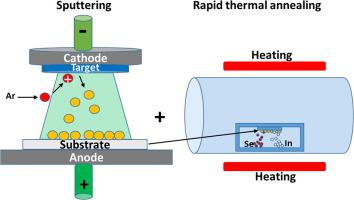
Abstract The undoped and indium doped SnSe (In-SnSe) thin films were successfully prepared by the two-stage process (sputtering and rapid thermal annealing process). The physical properties of the prepared thin films were investigated. Crystallographic patterns of the undoped and doped SnSe thin films showed the single-phase orthorhombic-SnSe. The diffraction peaks slightly shifted towards the higher diffraction angles as well as Raman peaks also shifted towards higher Raman shift by doping of indium. Morphology of the In-SnSe films changed significantly by changing the indium percentage. The optical bandgap of SnSe and In-SnSe films was varied in between 1.06 eV and 1.50 eV, and the electrical properties of In-SnSe films were significantly changed with dopant concentration. The obtained physical properties of In-SnSe thin films are suitable for solar cell device fabrication.
中文翻译:

用于光伏应用的铟 (In) 掺杂 SnSe 薄膜的开发
摘要 通过两步法(溅射和快速热退火工艺)成功制备了未掺杂和铟掺杂的SnSe(In-SnSe)薄膜。研究了制备的薄膜的物理性能。未掺杂和掺杂的 SnSe 薄膜的晶体图案显示单相正交-SnSe。通过掺杂铟,衍射峰略微向更高的衍射角移动,拉曼峰也向更高的拉曼位移移动。通过改变铟百分比,In-SnSe 薄膜的形态发生了显着变化。SnSe 和 In-SnSe 薄膜的光学带隙在 1.06 eV 和 1.50 eV 之间变化,并且 In-SnSe 薄膜的电性能随掺杂浓度而显着变化。
更新日期:2020-12-01
中文翻译:
用于光伏应用的铟 (In) 掺杂 SnSe 薄膜的开发
摘要 通过两步法(溅射和快速热退火工艺)成功制备了未掺杂和铟掺杂的SnSe(In-SnSe)薄膜。研究了制备的薄膜的物理性能。未掺杂和掺杂的 SnSe 薄膜的晶体图案显示单相正交-SnSe。通过掺杂铟,衍射峰略微向更高的衍射角移动,拉曼峰也向更高的拉曼位移移动。通过改变铟百分比,In-SnSe 薄膜的形态发生了显着变化。SnSe 和 In-SnSe 薄膜的光学带隙在 1.06 eV 和 1.50 eV 之间变化,并且 In-SnSe 薄膜的电性能随掺杂浓度而显着变化。


 京公网安备 11010802027423号