当前位置:
X-MOL 学术
›
J. Alloys Compd.
›
论文详情
Our official English website, www.x-mol.net, welcomes your
feedback! (Note: you will need to create a separate account there.)
Determination of band alignment in two-dimensional h-BN/WS2 van der waals heterojunction by X-ray photoelectron spectroscopy
Journal of Alloys and Compounds ( IF 5.8 ) Pub Date : 2021-02-01 , DOI: 10.1016/j.jallcom.2020.157301 Shu’an Xing , Guijuan Zhao , Yan Xu , Jie Wang , Xunshuan Li , Wenge Yang , Guipeng Liu , Jianhong Yang
Journal of Alloys and Compounds ( IF 5.8 ) Pub Date : 2021-02-01 , DOI: 10.1016/j.jallcom.2020.157301 Shu’an Xing , Guijuan Zhao , Yan Xu , Jie Wang , Xunshuan Li , Wenge Yang , Guipeng Liu , Jianhong Yang
|
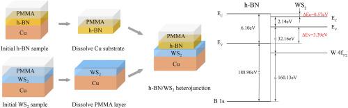
Abstract We have fabricated two-dimensional h-BN/WS2 van der Waals heterojunctions by stacking h-BN and WS2 monolayers, and experimentally measured the valence band offset (VBO) of h-BN/WS2 heterojunction by X-ray photoelectron spectroscopy (XPS). The h-BN and WS2 monolayers band gaps and the measured value of VBO were used to determine the conduction band offset (CBO). The measurement results of VBO and CBO are 3.39 ± 0.15 eV and 0.57 ± 0.15 eV, respectively, revealing a type-I band alignment. It is urgent to measure the band alignment parameters of h-BN/WS2 heterojunctions for analyzing and designing h-BN/WS2 based devices.
中文翻译:

通过 X 射线光电子能谱测定二维 h-BN/WS2 范德华异质结中的能带排列
摘要 我们通过堆叠 h-BN 和 WS2 单层制备了二维 h-BN/WS2 范德华异质结,并通过 X 射线光电子能谱 (XPS) 实验测量了 h-BN/WS2 异质结的价带偏移 (VBO)。 )。h-BN 和 WS2 单层带隙和 VBO 的测量值用于确定导带偏移 (CBO)。VBO 和 CBO 的测量结果分别为 3.39 ± 0.15 eV 和 0.57 ± 0.15 eV,表明 I 型带对齐。迫切需要测量 h-BN/WS2 异质结的能带对准参数,以分析和设计基于 h-BN/WS2 的器件。
更新日期:2021-02-01
中文翻译:
通过 X 射线光电子能谱测定二维 h-BN/WS2 范德华异质结中的能带排列
摘要 我们通过堆叠 h-BN 和 WS2 单层制备了二维 h-BN/WS2 范德华异质结,并通过 X 射线光电子能谱 (XPS) 实验测量了 h-BN/WS2 异质结的价带偏移 (VBO)。 )。h-BN 和 WS2 单层带隙和 VBO 的测量值用于确定导带偏移 (CBO)。VBO 和 CBO 的测量结果分别为 3.39 ± 0.15 eV 和 0.57 ± 0.15 eV,表明 I 型带对齐。迫切需要测量 h-BN/WS2 异质结的能带对准参数,以分析和设计基于 h-BN/WS2 的器件。


 京公网安备 11010802027423号