当前位置:
X-MOL 学术
›
J. Alloys Compd.
›
论文详情
Our official English website, www.x-mol.net, welcomes your
feedback! (Note: you will need to create a separate account there.)
Electro-sonical deposition of Sb2Se3 nanostructured films for optoelectronic applications
Journal of Alloys and Compounds ( IF 5.8 ) Pub Date : 2021-02-01 , DOI: 10.1016/j.jallcom.2020.157308 Behrouz Baghbanzadeh-Dezfuli , Farid Jamali-Sheini , Mohsen Cheraghizade
Journal of Alloys and Compounds ( IF 5.8 ) Pub Date : 2021-02-01 , DOI: 10.1016/j.jallcom.2020.157308 Behrouz Baghbanzadeh-Dezfuli , Farid Jamali-Sheini , Mohsen Cheraghizade
|
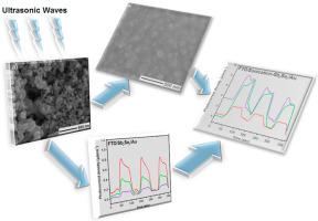
Abstract In this study, a film of antimony selenide (Sb2Se3) was deposited on the Fluorine-doped tin oxide (FTO) as a substrate via electrodeposition at the potential of −0.55 V and the temperature of 25 °C. The effect of ultrasound waves during electrodeposition was also investigated at different times. The structural, morphological, optical, optoelectronic, and temperature dependence of the electrical resistance of the samples was investigated. The results showed formation of the polycrystalline phase of orthorhombic Sb2Se3. It was observed that when the ultrasound waves were used, the crystallite size (grain) and energy band gap decreased. It was found that in samples with a specified configuration, the intensity of the photocurrent decreased with increasing deposition time. Additionally, the anodic and cathodic photocurrent behaviors of the samples depended on the type and location of the electrode connection. Furthermore, the electrical resistance of the samples decreased with increasing temperature. In the sample with the lowest deposition time, conductivity and electrical activation energy were reduced by applying ultrasound waves, but they were increased by increasing the deposition time.
中文翻译:

用于光电应用的 Sb2Se3 纳米结构薄膜的电声沉积
摘要 在这项研究中,在-0.55 V 的电位和25 °C 的温度下,通过电沉积在氟掺杂的氧化锡(FTO)上沉积了一层硒化锑(Sb2Se3)薄膜。还在不同时间研究了电沉积过程中超声波的影响。研究了样品电阻的结构、形态、光学、光电和温度依赖性。结果表明形成了正交晶系 Sb2Se3 的多晶相。观察到当使用超声波时,微晶尺寸(晶粒)和能带隙减小。发现在具有特定配置的样品中,光电流强度随着沉积时间的增加而降低。此外,样品的阳极和阴极光电流行为取决于电极连接的类型和位置。此外,样品的电阻随着温度的升高而降低。在沉积时间最短的样品中,施加超声波会降低电导率和电活化能,但随着沉积时间的增加,它们会增加。
更新日期:2021-02-01
中文翻译:
用于光电应用的 Sb2Se3 纳米结构薄膜的电声沉积
摘要 在这项研究中,在-0.55 V 的电位和25 °C 的温度下,通过电沉积在氟掺杂的氧化锡(FTO)上沉积了一层硒化锑(Sb2Se3)薄膜。还在不同时间研究了电沉积过程中超声波的影响。研究了样品电阻的结构、形态、光学、光电和温度依赖性。结果表明形成了正交晶系 Sb2Se3 的多晶相。观察到当使用超声波时,微晶尺寸(晶粒)和能带隙减小。发现在具有特定配置的样品中,光电流强度随着沉积时间的增加而降低。此外,样品的阳极和阴极光电流行为取决于电极连接的类型和位置。此外,样品的电阻随着温度的升高而降低。在沉积时间最短的样品中,施加超声波会降低电导率和电活化能,但随着沉积时间的增加,它们会增加。


 京公网安备 11010802027423号